
2026
Szary, Maciej J.; Jagiełło, Jakub; Reddig, Wiktoria; Dobrowolski, Artur; Ciuk, Tymoteusz; Prokopowicz, Rafał; Ziemba, Maciej; Wzorek, Marek; El-Ahmar, Semir
In: Physical Review Applied, vol. 26, iss. 3, pp. 034031, 2026.
@article{PRAppl2026_SA,
title = {Radiation-induced defect dynamics in two-dimensional/three-dimensional systems: A dimensionality advantage preserved within patterned graphene–SiC heterostructures},
author = {Maciej J. Szary and Jakub Jagiełło and Wiktoria Reddig and Artur Dobrowolski and Tymoteusz Ciuk and Rafał Prokopowicz and Maciej Ziemba and Marek Wzorek and Semir El-Ahmar},
doi = {10.1103/xdmg-zbky},
year = {2026},
date = {2026-09-15},
urldate = {2026-09-15},
journal = {Physical Review Applied},
volume = {26},
issue = {3},
pages = {034031},
abstract = {2D/3D heterostructures provide a powerful platform for uncovering how reduced dimensionality governs radiation response. While two-dimensional (2D) materials such as graphene, transition metal dichalcogenides, and MXenes have demonstrated notable structural resilience to radiation, fundamental differences in their radiation response compared with bulk three-dimensional (3D) crystals remain largely unverified. Here, we fabricate patterned 𝑎-Al2O3/graphene/H-intercalated SiC(0001) heterostructures and expose them to fast neutrons (1–2 MeV) across fluences from 1.9 ×10¹⁷ to 6.5×10¹⁸ n/cm2. The results reveal a striking disparity: despite the 3D environment, graphene accumulates damage 69–273 times more slowly than SiC, with its resilience further enhanced at high fluences due to early saturation, soft limited to only 0.0064% at 1.3 ×10¹⁹ n/cm2. This behavior is attributed to a two-channel defect accumulation model in 2D materials, involving interfacial evolution that dominates the early-stage response when the interface is chemically active, and direct lattice damage from atomic displacements, which persists but remains comparatively weak. These findings establish 2D lattices as fundamentally more radiation-resistant than 3D crystals and demonstrate that their advantages persist in realistic device architectures. Harnessing this resilience offers orders-of-magnitude improvements in structural stability for technologies operating under extreme irradiation, including fusion and fission reactors, particle accelerators, and aerospace systems.
Funding from the the Ministry of Science and Higher Education, Poland, under project No. 0512/SBAD/2620},
keywords = {},
pubstate = {published},
tppubtype = {article}
}
Funding from the the Ministry of Science and Higher Education, Poland, under project No. 0512/SBAD/2620

Kałuziak, Piotr; Raczyński, Jan; Majchrzycki, Łukasz; Szczęsny, Michał; Gawinkowski, Sylwester; Larowska-Zarych, Daria; El-Ahmar, Semir; Koczorowski, Wojciech
Raman Variability in CVD-Grown PtSe2 with Drop-Cast Gold Nanoparticles Conference
ECOSS 39, Oslo, September 1, 2026.
@conference{ECOSS2026_PK,

title = {Raman Variability in CVD-Grown PtSe2 with Drop-Cast Gold Nanoparticles},

author = {Piotr Kałuziak and Jan Raczyński and Łukasz Majchrzycki and Michał Szczęsny and Sylwester Gawinkowski and Daria Larowska-Zarych and Semir El-Ahmar and Wojciech Koczorowski},

url = {https://nano.put.poznan.pl/wp-content/uploads/2026/09/ECOSS39_2026_PK.pdf},

year  = {2026},

date = {2026-09-01},

booktitle = {ECOSS 39},

address = {Oslo, September 1},

abstract = {Funding from the Ministry of Science and Higher Education under project no. 0512/SPHD/2601.

Funding from the Ministry of Science and Higher Education under project no. 0512/SBAD/2620.},

keywords = {},

pubstate = {published},

tppubtype = {conference}

}
Funding from the Ministry of Science and Higher Education under project no. 0512/SBAD/2620.
Szary, Maciej J.; Jagiełło, Jakub; Reddig, Wiktoria; Dobrowolski, Artur; Ciuk, Tymoteusz; Prokopowicz, Rafał; Ziemba, Maciej; El-Ahmar, Semir
Impact of Intense Neutron Radiation: Two-Channel Damage Model of 2D/3D Heterostructure Conference
ECOSS 39, Oslo, August 31, 2026.
@conference{ECOSS2026_WR,

title = {Impact of Intense Neutron Radiation: Two-Channel Damage Model of 2D/3D Heterostructure},

author = {Maciej J. Szary and Jakub Jagiełło and Wiktoria Reddig and Artur Dobrowolski and Tymoteusz Ciuk and Rafał Prokopowicz and Maciej Ziemba and Semir El-Ahmar},

url = {https://nano.put.poznan.pl/wp-content/uploads/2026/09/ECOSS39_2026_WR.pdf},

year  = {2026},

date = {2026-08-31},

urldate = {2026-08-31},

booktitle = {ECOSS 39},

address = {Oslo, August 31},

abstract = {Funding from the Ministry of Science and Higher Education under project no. 0512/SBAD/6223.

Funding from the Ministry of Science and Higher Education under project no. 0512/SBAD/2620.},

keywords = {},

pubstate = {published},

tppubtype = {conference}

}
Funding from the Ministry of Science and Higher Education under project no. 0512/SBAD/2620.
Reddig, Wiktoria; Kałuziak, Piotr; Żebrowska, Agnieszka; Przychodnia, Marta; Ciuk, Tymoteusz; Piętak-Jurczak, Karolina; Szary, Maciej J.; Raczyński, Jan; Koczorowski, Wojciech; El-Ahmar, Semir
Monotonic High-Field Hall Response of Graphene Devices up to 11 T Journal Article
In: IEEE Electron Device Letters, vol. 47, no. 9, pp. 1906-1909, 2026.
@article{EDL2026,

title = {Monotonic High-Field Hall Response of Graphene Devices up to 11 T},

author = {Wiktoria Reddig and Piotr Kałuziak and Agnieszka Żebrowska and Marta Przychodnia and Tymoteusz Ciuk and Karolina Piętak-Jurczak and Maciej J. Szary and Jan Raczyński and Wojciech Koczorowski and Semir El-Ahmar},

doi = {10.1109/LED.2026.3702076},

year  = {2026},

date = {2026-07-06},

urldate = {2026-07-06},

journal = {IEEE Electron Device Letters},

volume = {47},

number = {9},

pages = {1906-1909},

abstract = {In strong magnetic fields, magnetoresistance can distort the transverse response of Hall devices and limit their usable field range. In this work, the high-field behavior of a graphene Hall device is compared with conventional, heavily donor-doped InSb Hall structures in magnetic fields up to 11 T at room and liquid-helium temperatures. The InSb samples exhibit non-monotonic transverse voltage characteristics associated with strong magnetoresistance, whereas the graphene device maintains a monotonic Hall response over the entire investigated field range. The transverse-voltage characteristics remain qualitatively unchanged between the two temperatures, indicating that the distortion in the InSb structures originates primarily from magnetotransport effects rather than temperature-dependent mechanisms. Our results demonstrate that graphene Hall devices preserve a distortion-free Hall response and low magnetoresistance (< 50 % at 11 T) in multi-tesla magnetic fields under both room-temperature and cryogenic conditions.


Funding from the the Ministry of Science and Higher Education, Poland, under project No. 0512/SBAD/2620

Funding from the National Centre for Research and Development under Grant Agreement No. LIDER/8/0021/L-11/19/NCBR/2020},

keywords = {},

pubstate = {published},

tppubtype = {article}

}
Funding from the the Ministry of Science and Higher Education, Poland, under project No. 0512/SBAD/2620
Funding from the National Centre for Research and Development under Grant Agreement No. LIDER/8/0021/L-11/19/NCBR/2020

Przychodnia, Marta; Drechsler, Alina; Bazarnik, Maciej; Schlenhoff, Anika
Single-atom Fe inclusions in MBE-grown monolayer MoS2/GR/Ir(111): an STM/STS study Conference
XII Polish Nanotechnology Conference (NANO 2026), Toruń, June 29 - July 3, 2026, (Oral presentation).
@conference{NANO2026_MP,

title = {Single-atom Fe inclusions in MBE-grown monolayer MoS2/GR/Ir(111): an STM/STS study},

author = {Marta Przychodnia and Alina Drechsler and Maciej Bazarnik and Anika Schlenhoff},

url = {https://nano.put.poznan.pl/wp-content/uploads/2026/07/NANO_2026_MP.pdf},

year  = {2026},

date = {2026-07-02},

urldate = {2026-07-02},

booktitle = {XII Polish Nanotechnology Conference (NANO 2026)},

address = {Toruń, June 29 - July 3},

abstract = {Transition metal dichalcogenides (TMDs) have attracted considerable interest due to their tunable electronic structure and strong sensitivity to defects in the two-dimensional limit. In monolayer TMDs, even low concentrations of vacancies, interstitials, or substitutional atoms can strongly modify local strain and the electronic density of states, providing opportunities for defect engineering of electronic, magnetic, optical, and catalytic properties. While most studies have focused on native defects in chemically grown materials, molecular beam epitaxy (MBE) enables controlled incorporation of designed atomic-scale impurities.

In this presentation, I discuss scanning tunneling microscopy and spectroscopy studiesof intentionally introduced Fe inclusions in MBE-grown monolayer MoS₂/Gr/Ir(111), realized by co-evaporation of Fe during growth. The Fe-related defects are identified through comparison with intrinsic defects observed previously in undoped MoS₂grown in the same UHV chamber. Differential conductance spectroscopy reveals impurityinduced in-gap states associated with Fe incorporation, while bias-dependent conductance mapping resolves their spatial structure. Resonant tunneling spectroscopy further shows that Fe inclusions modify image potential states, shifting their energetic positions through local variations of the work function. These results demonstrate controlled atomic impurity engineering in MBE-grown TMDs and its impact on the local electronic structure.


Funding from the Ministry of Science and Higher Education (Poland) within Project 0512/SBAD/2620.},

note = {Oral presentation},

keywords = {},

pubstate = {published},

tppubtype = {conference}

}
In this presentation, I discuss scanning tunneling microscopy and spectroscopy studiesof intentionally introduced Fe inclusions in MBE-grown monolayer MoS₂/Gr/Ir(111), realized by co-evaporation of Fe during growth. The Fe-related defects are identified through comparison with intrinsic defects observed previously in undoped MoS₂grown in the same UHV chamber. Differential conductance spectroscopy reveals impurityinduced in-gap states associated with Fe incorporation, while bias-dependent conductance mapping resolves their spatial structure. Resonant tunneling spectroscopy further shows that Fe inclusions modify image potential states, shifting their energetic positions through local variations of the work function. These results demonstrate controlled atomic impurity engineering in MBE-grown TMDs and its impact on the local electronic structure.
Funding from the Ministry of Science and Higher Education (Poland) within Project 0512/SBAD/2620.
Raczyński, Jan; Nowicki, Marek; Costina, I; Kot, Dawid; Koczorowski, Wojciech
Analysis of chemical phases formed in thin-film metal PtSe2 interfaces Conference
XII Polish Nanotechnology Conference (NANO 2026), Toruń, June 29 - July 3, 2026, (Oral presentation).
@conference{NANO2026_JR,

title = {Analysis of chemical phases formed in thin-film metal PtSe2 interfaces},

author = {Jan Raczyński and Marek Nowicki and I Costina and Dawid Kot and Wojciech Koczorowski},

url = {https://nano.put.poznan.pl/wp-content/uploads/2026/07/NANO_2026_JR.pdf},

year  = {2026},

date = {2026-07-01},

booktitle = {XII Polish Nanotechnology Conference (NANO 2026)},

address = {Toruń, June 29 - July 3},

abstract = {The continued miniaturization of electronic devices and the search for alternative systems to complement dominant silicon-based technologies are driving intense research into two-dimensional (2D) materials. This class of systems, pioneered by the discovery of graphene, now includes a broad range of materials including topological insulators, transition metal dichalcogenides (TMDs),and hexagonal boron nitride (h-BN). Among these, platinum diselenide (PtSe2), is emerging as a particularly promising TMD material due to its high theoretical charge carrier mobility surface chemical stability, and tunable energy bandgap.

From the application perspective, a comprehensive materials analysis must extend beyond the intrinsic properties of the material to include physicochemical interactions at the interfaces with other components of the device structure. This presentation will discuss in detail the investigations of thin-film metal (e.g., Ti, Cr, Ni, Pt)/PtSe2 interfaces, using Raman and X-ray Photoemission spectroscopy (XPS). These techniques allow for the determination of the chemical composition of the mixed phases formed at the interface and an evaluation of the thermal stability of such systems. Furthermore, complementary microscopic analyses (AFM and SEM) provide insights into surface morphology, features that are fundamental to the successful integration of these systems into next-generation electronic devices.


Funding from the National Science Centre, Grant No. 2019/35/0/ST5/01940.

Funding from the Polish National Agency for Academic Exchange, grant No. PPN/STA/2021/1/00043.

Funding from the Ministry of Education and Science (Poland) under Project No. 0512/SBAD/2620.},

note = {Oral presentation},

keywords = {},

pubstate = {published},

tppubtype = {conference}

}
From the application perspective, a comprehensive materials analysis must extend beyond the intrinsic properties of the material to include physicochemical interactions at the interfaces with other components of the device structure. This presentation will discuss in detail the investigations of thin-film metal (e.g., Ti, Cr, Ni, Pt)/PtSe2 interfaces, using Raman and X-ray Photoemission spectroscopy (XPS). These techniques allow for the determination of the chemical composition of the mixed phases formed at the interface and an evaluation of the thermal stability of such systems. Furthermore, complementary microscopic analyses (AFM and SEM) provide insights into surface morphology, features that are fundamental to the successful integration of these systems into next-generation electronic devices.
Funding from the National Science Centre, Grant No. 2019/35/0/ST5/01940.
Funding from the Polish National Agency for Academic Exchange, grant No. PPN/STA/2021/1/00043.
Funding from the Ministry of Education and Science (Poland) under Project No. 0512/SBAD/2620.
Kałuziak, Piotr; Raczyński, Jan; Majchrzycki, Łukasz; Szczęsny, Michał; Gawinkowski, Sylwester; Larowska-Zarych, Daria; El-Ahmar, Semir; Koczorowski, Wojciech
CTAB vs signal: why AuNPs do not enhance Raman response of PtSe2 in drop-cast systems Conference
XII Polish Nanotechnology Conference (NANO 2026), Toruń, June 29 - July 3, 2026, (Oral presentation).
@conference{NANO2026_PK,

title = {CTAB vs signal: why AuNPs do not enhance Raman response of PtSe2 in drop-cast systems },

author = {Piotr Kałuziak and Jan Raczyński and Łukasz Majchrzycki and Michał Szczęsny and Sylwester Gawinkowski and Daria Larowska-Zarych and Semir El-Ahmar and Wojciech Koczorowski},

url = {https://nano.put.poznan.pl/wp-content/uploads/2026/07/NANO_2026_PK.pdf},

year  = {2026},

date = {2026-06-30},

urldate = {2026-06-30},

booktitle = {XII Polish Nanotechnology Conference (NANO 2026)},

address = {Toruń, June 29 - July 3},

abstract = {Plasmonic modification of Raman response using gold nanoparticles (AuNPs) is widely investigated as a strategy to enhance sensitivity in two-dimensional (2D) material systems [1,2]. Such hybrid platforms are considered for applications requiring spatially heterogeneous spectral responses, including Physical Unclonable Features (PUFs).

In this work, we examine the Raman response of PtSe₂ modified with AuNPs deposited via drop casting, focusing on the mutual interaction between plasmonic effects and nanoparticle surface chemistry. Contrary to expectations, no clear enhancement of characteristic PtSe₂ Raman modes is observed. Instead, the spectra exhibit additional low-frequency features, which can be attributed to ligandrelated vibrations or Au–halide interactions associated with CTAB-stabilized nanoparticles [3–4]. Spatially resolved Raman mapping reveals that these contributions are highly localized and correlate with nanoparticle-rich regions, indicating that surface chemistry can dominate over electromagnetic enhancement. As a result, the presence of AuNPs leads to modification and, in some cases, masking of the PtSe₂ spectral response rather than its amplification. These findings highlight a key limitation of CTAB capped AuNPs in drop-cast configurations for Surface-Enhanced Raman Spectroscopy (SERS) studies of 2D materials. The results highlight the key role of ligand chemistry in determining the observed signal.


Funding from the Ministry of Education and Science (Poland) under Project No. 0512/SBAD/2620 and the PhDBoost Program (No. 0512/SPHD/2601).},

note = {Oral presentation},

keywords = {},

pubstate = {published},

tppubtype = {conference}

}
In this work, we examine the Raman response of PtSe₂ modified with AuNPs deposited via drop casting, focusing on the mutual interaction between plasmonic effects and nanoparticle surface chemistry. Contrary to expectations, no clear enhancement of characteristic PtSe₂ Raman modes is observed. Instead, the spectra exhibit additional low-frequency features, which can be attributed to ligandrelated vibrations or Au–halide interactions associated with CTAB-stabilized nanoparticles [3–4]. Spatially resolved Raman mapping reveals that these contributions are highly localized and correlate with nanoparticle-rich regions, indicating that surface chemistry can dominate over electromagnetic enhancement. As a result, the presence of AuNPs leads to modification and, in some cases, masking of the PtSe₂ spectral response rather than its amplification. These findings highlight a key limitation of CTAB capped AuNPs in drop-cast configurations for Surface-Enhanced Raman Spectroscopy (SERS) studies of 2D materials. The results highlight the key role of ligand chemistry in determining the observed signal.
Funding from the Ministry of Education and Science (Poland) under Project No. 0512/SBAD/2620 and the PhDBoost Program (No. 0512/SPHD/2601).
Szary, Maciej J.; Jagiełło, Jakub; Reddig, Wiktoria; Dobrowolski, Artur; Ciuk, Tymoteusz; Prokopowicz, Rafał; Ziemba, Maciej; El-Ahmar, Semir
Two-channel damage model in 2D/3D heterostructures under high energy neutrons Conference
XII Polish Nanotechnology Conference (NANO 2026), Toruń, June 29 - July 3, 2026, (Oral presentation).
@conference{NANO2026_WR,

title = {Two-channel damage model in 2D/3D heterostructures under high energy neutrons},

author = {Maciej J. Szary and Jakub Jagiełło and Wiktoria Reddig and Artur Dobrowolski and Tymoteusz Ciuk and Rafał Prokopowicz and Maciej Ziemba and Semir El-Ahmar},

url = {https://nano.put.poznan.pl/wp-content/uploads/2026/07/NANO_2026_WR.pdf},

year  = {2026},

date = {2026-06-30},

booktitle = {XII Polish Nanotechnology Conference (NANO 2026)},

address = {Toruń, June 29 - July 3},

abstract = {Materials with reduced dimensionality suppress collision cascades from neutron radiation that is responsible for defect accumulation in bulk materials. Therefore, understanding radiation damage in 2-dimensional systems iscritical for the next-generation of radiation-tolerant electronics operating in extreme environments like future fusion reactors or space technologies. The question remains, does reduced dimensionality retains its advantage while a part of a 3D structure? In this study, we examine a-Al2O3/graphene/Hintercalated SiC heterostructures subjected to 1—2 MeV neutronradiation up to 6.5 x 10¹⁸ n/cm2, focusing on how reduced dimensionality responds to defect formation within a realistic 2D/3D architecture. Despite thesurrounding bulk environment, graphene shows 69 —273 times lower damagethan SiC and reaches an early soft saturation. Hall-effect measurements reveal a radiation-driven transition from p- to n-type conductivity,indicating progressive hydrogen depletion [5]. These observations aresupported by Density Functional Theory (OFT) calculations, which link interfacial chemical evolution to the emergence of disorder without requiring significant lattice displacement [5, 6].

We interpret these results through a two-channel damage model: (i) interfacial evolution dominating defect formation in 2D layer, and (ii) direct lattice damage that is prominent in the bulk. This framework highlights the decisive role of interface chemistry and provides a pathway for engineering radiation-resistant 2D/3D heterostructures.


Funding from the Ministry of Science and Higher Education (Poland) within project no. 0512/SBAD/2620 and 0512/SBAD/6223.},

note = {Oral presentation},

keywords = {},

pubstate = {published},

tppubtype = {conference}

}
We interpret these results through a two-channel damage model: (i) interfacial evolution dominating defect formation in 2D layer, and (ii) direct lattice damage that is prominent in the bulk. This framework highlights the decisive role of interface chemistry and provides a pathway for engineering radiation-resistant 2D/3D heterostructures.
Funding from the Ministry of Science and Higher Education (Poland) within project no. 0512/SBAD/2620 and 0512/SBAD/6223.

Raczyński, Jan; Szczęsny, Michał; El-Ahmar, Semir; Chłopocka, Edyta; Szybowicz, Mirosław; Kot, Dawid; Koczorowski, Wojciech
Thermally Induced Correlation Effects in metal/PtSe2 heterostructures studied by Raman Spectroscopy Conference
PUT STEM DAY 2026, Poznań, May 15, 2026, (Poster presentation).
@conference{PUTSTEM2026_JR,

title = {Thermally Induced Correlation Effects in metal/PtSe2 heterostructures studied by Raman Spectroscopy},

author = {Jan Raczyński and Michał Szczęsny and Semir El-Ahmar and Edyta Chłopocka and Mirosław Szybowicz and Dawid Kot and Wojciech Koczorowski},

url = {https://nano.put.poznan.pl/wp-content/uploads/2026/05/PUTSTEM2026_MS.pdf},

year  = {2026},

date = {2026-05-15},

booktitle = {PUT STEM DAY 2026},

address = {Poznań, May 15},

abstract = {We present a systematic study of interfacial physics in meta/PtSe2 heterostructures (metal = Ti, Cr, Ni, Pd, Pt) employing temperature-dependent Raman spectroscopy (RT–473 K) and SEM imaging. The deposition of metallic overlayers with thicknesses of 10 and 15 nm results in a pronounced narrowing of phonon linewidths (up to 50%) and a significant increase in the IA1g/IEg intensity ratio compared to bulk PtSe2. These effects are attributed to dielectric screening and work-function-dependent charge redistribution. An analysis of the relationship between the Eg and A1g phonon modes indicates that the introduction of metallic layers leads to the onset of compressive strain and charge carrier doping. At the same time, the inherent anharmonic behaviour of the lattice captured by the temperature-dependent coefficients remains largely unaffected and closely matches that observed in bulk PtSe₂. Furthermore, although annealing triggers metaldependent morphological modifications, the core vibrational properties of the PtSe2 lattice remain essentially unchanged. These findings provide insight into the electronic and mechanical coupling at metal–2D interfaces and highlight PtSe2 as a robust platform for stable two-dimensional electronic applications.},

note = {Poster presentation},

keywords = {},

pubstate = {published},

tppubtype = {conference}

}
Reddig, Wiktoria; Kałuziak, Piotr; Żebrowska, Agnieszka; Przychodnia, Marta; Ciuk, Tymoteusz; Piętak-Jurczak, Karolina; Szary, Maciej J.; Raczyński, Jan; Koczorowski, Wojciech; El-Ahmar, Semir
High-field galvanomagnetic response of graphene and InSb-based hallotrons Conference
PUT STEM DAY 2026, Poznań, May 15, 2026, (Poster presentation).
@conference{PUTSTEM2026_WR,

title = {High-field galvanomagnetic response of graphene and InSb-based hallotrons},

author = {Wiktoria Reddig and Piotr Kałuziak and Agnieszka Żebrowska and Marta Przychodnia and Tymoteusz Ciuk and Karolina Piętak-Jurczak and Maciej J. Szary and Jan Raczyński and Wojciech Koczorowski and Semir El-Ahmar},

url = {https://nano.put.poznan.pl/wp-content/uploads/2026/05/PUTSTEM2026_WR.pdf},

year  = {2026},

date = {2026-05-15},

urldate = {2026-05-15},

booktitle = {PUT STEM DAY 2026},

address = {Poznań, May 15},

abstract = {Emerging technologies such as fusion energy systems and space applications increasingly demand electronic components capable of stable and predictable operation in multi-tesla magnetic fields over wide

temperature ranges. Semiconductor Hall devices, particularly those based on InSb, are widely used in demanding conditions due to their high carrier mobility and sensitivity. Controlled donor doping enables

stabilization of electrical properties over broad temperatures. However, it simultaneously alters intrinsic transport properties and introduces trade-offs between sensitivity, thermal stability, and reproducibility. As

a result, device performance may deviate from ideal behavior in strong magnetic fields. These limitations motivate the exploration of alternative materials for robust magnetic-field sensing, with graphene emerging as a promising candidate. In this work, we present a comparative study of galvanomagnetic properties of two types of deviceready Hall sensor platforms: (i) p-type hydrogen-intercalated quasi-free-standing epitaxial graphene grown on 4H-SiC(0001) passivated with an Al2O3, and (ii) heavily donor-doped InSb thin film deposited on semi-insulating GaAs substrate and protected with dielectric layer. Both device types were integrated into CERDIP8 ceramic housing, ensuring suitability for operation in harsh environments. InSb structures with different doping levels were analysed to show the impact of transport properties on electrical response in strong magnetic field. The galvanomagnetic response was investigated in magnetic fields up to 11 T at room temperature and under liquid-helium conditions. The graphene-based devices exhibit a monotonic and nearly linear Hall response across the full magnetic-field range, indicating weak magnetoresistive effects. In contrast, InSbbased sensors, due to intense doping, display significant nonlinearity and distortion in the transverse voltage at high magnetic fields. This effect originates from strong magnetoresistance, where the rapid increase of longitudinal resistance leads to mixing between longitudinal and transverse voltage components, distorting the Hall signal [4]. As a result, the usable magnetic-field range of semiconductor Hall devices becomes limited in the multi-tesla regime. The results demonstrate that graphene Hall devices maintain superior stability of response under high magnetic field and cryogenic conditions. These findings highlight graphene as a promising material platform for reliable magnetic-field sensing in extreme environments where conventional semiconductorbased Hall sensors, such as InSb, may face intrinsic limitations.


Funding from the Ministry of Science and Higher Education under project no. 0512/SPHD/2501.

Funding from the Ministry of Science and Higher Education under project no. 0512/SBAD/2620.

Funding from National Centre for Research and Development under Grant Agreement No. LIDER/8/0021/L-11/19/NCBR/2020.},

note = {Poster presentation},

keywords = {},

pubstate = {published},

tppubtype = {conference}

}
temperature ranges. Semiconductor Hall devices, particularly those based on InSb, are widely used in demanding conditions due to their high carrier mobility and sensitivity. Controlled donor doping enables
stabilization of electrical properties over broad temperatures. However, it simultaneously alters intrinsic transport properties and introduces trade-offs between sensitivity, thermal stability, and reproducibility. As
a result, device performance may deviate from ideal behavior in strong magnetic fields. These limitations motivate the exploration of alternative materials for robust magnetic-field sensing, with graphene emerging as a promising candidate. In this work, we present a comparative study of galvanomagnetic properties of two types of deviceready Hall sensor platforms: (i) p-type hydrogen-intercalated quasi-free-standing epitaxial graphene grown on 4H-SiC(0001) passivated with an Al2O3, and (ii) heavily donor-doped InSb thin film deposited on semi-insulating GaAs substrate and protected with dielectric layer. Both device types were integrated into CERDIP8 ceramic housing, ensuring suitability for operation in harsh environments. InSb structures with different doping levels were analysed to show the impact of transport properties on electrical response in strong magnetic field. The galvanomagnetic response was investigated in magnetic fields up to 11 T at room temperature and under liquid-helium conditions. The graphene-based devices exhibit a monotonic and nearly linear Hall response across the full magnetic-field range, indicating weak magnetoresistive effects. In contrast, InSbbased sensors, due to intense doping, display significant nonlinearity and distortion in the transverse voltage at high magnetic fields. This effect originates from strong magnetoresistance, where the rapid increase of longitudinal resistance leads to mixing between longitudinal and transverse voltage components, distorting the Hall signal [4]. As a result, the usable magnetic-field range of semiconductor Hall devices becomes limited in the multi-tesla regime. The results demonstrate that graphene Hall devices maintain superior stability of response under high magnetic field and cryogenic conditions. These findings highlight graphene as a promising material platform for reliable magnetic-field sensing in extreme environments where conventional semiconductorbased Hall sensors, such as InSb, may face intrinsic limitations.
Funding from the Ministry of Science and Higher Education under project no. 0512/SPHD/2501.
Funding from the Ministry of Science and Higher Education under project no. 0512/SBAD/2620.
Funding from National Centre for Research and Development under Grant Agreement No. LIDER/8/0021/L-11/19/NCBR/2020.
Kwiecień, Katarzyna; Kałuziak, Piotr; Raczyński, Jan; Puchalska, Agnieszka; Dychalska, Anna; Chłopocka, Edyta; Kot, Dawid; Majchrzycki, Łukasz; Szybowicz, Mirosław; Jurczyszyn, Leszek; Dobrotvorska, Mariya V.; Lewandowski, Mikołaj; Koczorowski, Wojciech
An experimental study of bulk HfS2, ZrS2 and HfSe2 monocrystal surfaces exposed to ambient air Conference
PUT STEM DAY 2026, Poznań, May 15, 2026, (Oral presentation).
@conference{PUTSTEM2026_KK,

title = {An experimental study of bulk HfS2, ZrS2 and HfSe2 monocrystal surfaces exposed to ambient air},

author = {Katarzyna Kwiecień and Piotr Kałuziak and Jan Raczyński and Agnieszka Puchalska and Anna Dychalska and Edyta Chłopocka and Dawid Kot and Łukasz Majchrzycki and Mirosław Szybowicz and Leszek Jurczyszyn and Mariya V. Dobrotvorska and Mikołaj Lewandowski and Wojciech Koczorowski},

url = {https://nano.put.poznan.pl/wp-content/uploads/2026/05/PUTSTEM2026_KK.pdf},

year  = {2026},

date = {2026-05-15},

urldate = {2026-05-15},

booktitle = {PUT STEM DAY 2026},

address = {Poznań, May 15},

abstract = {HfS2, ZrS2, and HfSe2 belong to the group IV transition metal dichalcogenides (TMDs). These materials are promising for next-generation electronics due to their tunable band gaps (1–2 eV) and high

predicted carrier mobilities at room temperature. While many TMDs are chemically inert, group IV TMDs oxidize when exposed to air. Understanding how this oxidation affects their physical properties and

surface morphology is critical for their use in electronic devices. In this study, we investigate bulk HfS2 and ZrS2 monocrystals exposed to ambient air and compare our findings to the observations we made for the oxidized HfSe2. Scanning electron microscopy (SEM) and atomic force microscopy (AFM) images reveal clear differences in surface morphology: HfSe2 develops characteristic selenium-rich blisters, while the sulfur-based TMDs (HfS2 and ZrS2) show the formation of pits with electronic and mechanical properties that differ from those of the surrounding area. Further Raman spectroscopy data reveals that HfSe₂ vibrational modes change rapidly due to the ambient air exposure of the material, whereas the vibrational properties of HfS2 and ZrS2 remain stable. Finally, Xray photoemission spectroscopy (XPS) and energy-dispersive X-ray spectroscopy (EDX) show that the sulfur-based TMDs are significantly more chemically stable in ambient air than HfSe2. These results offer a comprehensive description of the surface oxidation of chosen TMDs, which is crucial in the context of the material selection and technological processing requirements for future group IV TMD-based devices.


Funding from the Ministry of Science and Higher Education under project no. 0512/SBAD/6220.

Funding from the Ministry of Science and Higher Education under project no. 0512/SBAD/2620.},

note = {Oral presentation},

keywords = {},

pubstate = {published},

tppubtype = {conference}

}
predicted carrier mobilities at room temperature. While many TMDs are chemically inert, group IV TMDs oxidize when exposed to air. Understanding how this oxidation affects their physical properties and
surface morphology is critical for their use in electronic devices. In this study, we investigate bulk HfS2 and ZrS2 monocrystals exposed to ambient air and compare our findings to the observations we made for the oxidized HfSe2. Scanning electron microscopy (SEM) and atomic force microscopy (AFM) images reveal clear differences in surface morphology: HfSe2 develops characteristic selenium-rich blisters, while the sulfur-based TMDs (HfS2 and ZrS2) show the formation of pits with electronic and mechanical properties that differ from those of the surrounding area. Further Raman spectroscopy data reveals that HfSe₂ vibrational modes change rapidly due to the ambient air exposure of the material, whereas the vibrational properties of HfS2 and ZrS2 remain stable. Finally, Xray photoemission spectroscopy (XPS) and energy-dispersive X-ray spectroscopy (EDX) show that the sulfur-based TMDs are significantly more chemically stable in ambient air than HfSe2. These results offer a comprehensive description of the surface oxidation of chosen TMDs, which is crucial in the context of the material selection and technological processing requirements for future group IV TMD-based devices.
Funding from the Ministry of Science and Higher Education under project no. 0512/SBAD/6220.
Funding from the Ministry of Science and Higher Education under project no. 0512/SBAD/2620.
Shuryhin, Fedir; Biliak, Roman; Liakh-Kaguy, Natalia; Kost, Yaroslav; Sukhorebryi, Serhii; El-Ahmar, Semir; Ciuk, Tymoteusz
Investigation of Hall Sensors Based on QFS Graphene in a 1-T Magnetic Field Journal Article
In: IEEE Sensors Journal, vol. 26, no. 11, pp. 16825 - 16833, 2026.
@article{IEEEsens2026_SA,

title = {Investigation of Hall Sensors Based on QFS Graphene in a 1-T Magnetic Field},

author = {Fedir Shuryhin and Roman Biliak and Natalia Liakh-Kaguy and Yaroslav Kost and Serhii Sukhorebryi and Semir El-Ahmar and Tymoteusz Ciuk},

doi = {10.1109/JSEN.2026.3685161},

year  = {2026},

date = {2026-04-23},

journal = {IEEE Sensors Journal},

volume = {26},

number = {11},

pages = {16825 - 16833},

abstract = {This article presents the results of an experimental study of advanced Hall sensors made of quasi-free-standing (QFS) graphene on 4H-SiC in a magnetic field up to ±1 T. The purpose was to evaluate the current-mode sensitivity and linearity of such sensors in moderate magnetic fields in the context of their potential use in diagnostics and control systems for magnetic confinement fusion reactors. The sensors utilize epitaxial chemical vapor deposition (CVD) graphene on hydrogen-terminated 5-keV H+-modified semi-insulating (SI) on-axis 4H-SiC(0001). We describe the use of the rotating current method to eliminate parasitic signal shift. The dependence of the sensors’ Hall signal on the magnetic field is linear with an error not exceeding 0.12%, which indicates high measurement accuracy. A close-to-quadratic dependence of the parasitic offset voltage and surface resistance on the magnetic field is also witnessed, which is likely associated with the manifestation of the magnetoresistive effect. The results of the study confirm the prospects of using graphene-on-SiC Hall sensors in moderate magnetic fields up to ±1 T.


Funding from the Ministry of Education and Science (Poland), Project No. 0512/SBAD/2620},

keywords = {},

pubstate = {published},

tppubtype = {article}

}
Funding from the Ministry of Education and Science (Poland), Project No. 0512/SBAD/2620
Leśniewski, Bartosz; Szczurek, Anna; Simon, Paul; Nowacki, Krzysztof; Kubacki, Jerzy; Matczak, Michał; Kuświk, Piotr; Nowicki, Marek; Kubiak, Anita; Kotula, Martyna; Souiba, Zineb; Ehrlich, Hermann
Functionalization of sustainable biomaterial spongin through creating new 3D composites with chromium for catalytic applications Journal Article
In: Discover Materials, vol. 6, no. 196, 2026.
@article{ADVMAT2026,

title = {Functionalization of sustainable biomaterial spongin through creating new 3D composites with chromium for catalytic applications},

author = {Bartosz Leśniewski and Anna Szczurek and Paul Simon and Krzysztof Nowacki and Jerzy Kubacki and Michał Matczak and Piotr Kuświk and Marek Nowicki and Anita Kubiak and Martyna Kotula and Zineb Souiba and Hermann Ehrlich},

doi = {10.1007/s43939-026-00651-1},

year  = {2026},

date = {2026-04-11},

journal = {Discover Materials},

volume = {6},

number = {196},

abstract = {The structural biocomposite spongin, which forms three-dimensional (3D) microporous skeletons in keratosan demosponges, known as the first multicellular organisms, belongs to sustainable biological materials. This study reports the first chromium tanning of spongin scaffolds isolated from two species of industrially used commercial sponges (Hippospongia communis and Spongia tampa) under extreme biomimetic conditions. Carbonization of the studied spongin samples followed by chromium plating led to the formation of complex multiphase structures never reported before. We use digital, and scanning electron microscopy, as well as XRD, FT-IR, XPS, thermogravimetric analysis and HR-TEM, for identification and characterization of the created 3D spongin-chromium composites. A mechanism for the interaction of chromium with the functional groups of spongin has also been proposed. Our data provide insights into the highly specific chemical and structural arrangements resulting from the Cr-tanning of diverse forms of spongin-based composite materials with perspectives of their practical applications including the hydrogen evolution reaction.},

keywords = {},

pubstate = {published},

tppubtype = {article}

}

El-Ahmar, Semir; Jankowski, Jakub; Przychodnia, Marta; Reddig, Wiktoria; Kałuziak, Piotr; Raczyński, Jan; Czaja, Paweł
Czujnik pola magnetycznego oparty na efekcie Halla do pracy w zakresie temperatur 5 K–650 K Patent
2026, (Patent application P.455399).
@patent{P.455399_SA,

title = {Czujnik pola magnetycznego oparty na efekcie Halla do pracy w zakresie temperatur 5 K–650 K},

author = {Semir El-Ahmar and Jakub Jankowski and Marta Przychodnia and Wiktoria Reddig and Piotr Kałuziak and Jan Raczyński and Paweł Czaja},

year  = {2026},

date = {2026-04-10},

urldate = {2026-04-10},

note = {Patent application P.455399},

keywords = {},

pubstate = {published},

tppubtype = {patent}

}
Kałuziak, Piotr; Raczyński, Jan; El-Ahmar, Semir; Przychodnia, Marta; Nowicki, Marek; Czajka, Ryszard; Koczorowski, Wojciech
Material-based uniqueness in InSb thin films: Flash Evaporation Epitaxy as a tool for secure device engineering Journal Article
In: Vacuum, vol. 247, pp. 115166, 2026.
@article{Vacuum_PK2026,

title = {Material-based uniqueness in InSb thin films: Flash Evaporation Epitaxy as a tool for secure device engineering},

author = {Piotr Kałuziak and Jan Raczyński and Semir El-Ahmar and Marta Przychodnia and Marek Nowicki and Ryszard Czajka and Wojciech Koczorowski},

doi = {10.1016/j.vacuum.2026.115166},

year  = {2026},

date = {2026-02-07},

urldate = {2026-02-07},

journal = {Vacuum},

volume = {247},

pages = {115166},

abstract = {In this work, we investigate Flash Evaporation Epitaxy (FEE) as a method for fabricating InSb/GaAs heterostructures exhibiting intrinsic electrical variability while preserving structural and chemical homogeneity. n-InSb/i-GaAs systems were grown using a modified FEE-based high-vacuum setup. The elemental mapping in both the plan view and the cross-section shows a close stoichiometric distribution of the antimony and indium atoms, and a homogeneous incorporation of oxygen with a low content at a level of 1 at.%. SEM and AFM analyses confirm a uniform surface morphology. Electrical characterisation of full wafers and progressively structured areas reveals variations in sheet resistance with the range of X-Y exceeding experimental uncertainty. These variations form a statistical distribution of electrical parameters resulting from the properties of the FEE method rather than from significant structural or stoichiometry non-uniformity. This distribution defines the material-based uniqueness of the films. While usually considered a limitation, it is demonstrated here as a functional advantage for generating unique physical signatures applicable to hardware-level authenticity-verification systems.


Funding from the Ministry of Education and Science (Poland), Project No. 0512/SBAD/2520 and 0512/SBAD/6217

Funding from the National Centre for Research and Development (Poland), Project “MAGSET” No. LIDER/8/0021/L- 11/19/NCBR/2020},

keywords = {},

pubstate = {published},

tppubtype = {article}

}
Funding from the Ministry of Education and Science (Poland), Project No. 0512/SBAD/2520 and 0512/SBAD/6217
Funding from the National Centre for Research and Development (Poland), Project “MAGSET” No. LIDER/8/0021/L- 11/19/NCBR/2020
Kałużny, Jarosław; Wojciechowski, Łukasz; Runka, Tomasz; Boncel, Sławomir; Marek, Adam A.; Grochalski, Karol; Gapiński, Bartosz; Skrzypek, Magdalena; Nowicki, Marek; Błaszkiewicz, Paulina; Terzyk, Artur P.; Giedrowicz, Marcin
Minimal metal-CNT-enrichment for maximal lubricity gain: boosting lithium grease performance for general applications Journal Article
In: Carbon, vol. 248, pp. 121187, 2026.
@article{Carbon_MN2026,

title = {Minimal metal-CNT-enrichment for maximal lubricity gain: boosting lithium grease performance for general applications},

author = {Jarosław Kałużny and Łukasz Wojciechowski and Tomasz Runka and Sławomir Boncel and Adam A. Marek and Karol Grochalski and Bartosz Gapiński and Magdalena Skrzypek and Marek Nowicki and Paulina Błaszkiewicz and Artur P. Terzyk and Marcin Giedrowicz

},

doi = {10.1016/j.carbon.2025.121187},

year  = {2026},

date = {2026-02-05},

journal = {Carbon},

volume = {248},

pages = {121187},

abstract = {Frictional losses in mechanical systems consume ∼23% of global energy, demanding advanced, scalable lubrication solutions. We present high-performance nanolubricants by incorporating trace amounts (0.01 wt%) of gold-, copper-, or nickel-multi-walled carbon nanotube (MWCNT) hybrids into a commercial lithium soap grease. In four-ball tribometer tests, Cu-MWCNTs achieved a 75% reduction in wear scar diameter (from 2.96 mm to 0.73 mm at 1 kN load) and raised the maximum non-seizure load from 1.2 kN to beyond 1.4 kN. A tenfold increase in nanomaterial concentration (0.1 wt%) slightly reduced performance, revealing a non-monotonic concentration–efficacy relationship. Extended bearing tests over 1,150 h (∼152 million revolutions) confirmed long-term durability. Raman spectroscopy showed MWCNT persistence in rolling contacts, whereas under sliding, they transformed into amorphous carbon, serving a sacrificial role. No copper residues were detected via energy-dispersive X-ray spectroscopy (EDS), suggesting a catalytic – not depositional – tribochemical function. Cu-MWCNTs synergistically enhanced zinc dialkyldithiophosphate (ZDDP) tribofilm formation and inhibited steel oxidation under high-load friction. These findings demonstrate that trace-level, surface-engineered carbon nanomaterials can significantly improve lubricant performance through complex mechanochemical interactions. The developed nanolubricants offer a scalable, energy-efficient solution fully compatible with existing industrial greases and testing protocols.},

keywords = {},

pubstate = {published},

tppubtype = {article}

}
Mituła-Chmielowiec, Katarzyna; Januszewski, Rafał; Nowicki, Marek; Dudziec, Beata
When Flexibility Meets Rigidity: Unlocking the Potential of Polysiloxane–Silsesquioxane Hybrids Journal Article
In: Polymer, vol. 347, pp. 129679, 2026.
@article{Polymer_MN2026,

title = {When Flexibility Meets Rigidity: Unlocking the Potential of Polysiloxane–Silsesquioxane Hybrids},

author = {Katarzyna Mituła-Chmielowiec and Rafał Januszewski and Marek Nowicki and Beata Dudziec},

doi = {10.1016/j.polymer.2026.129679},

year  = {2026},

date = {2026-01-30},

urldate = {2026-01-30},

journal = {Polymer},

volume = {347},

pages = {129679},

abstract = {Hybrid polysiloxanes (PS) incorporating silsesquioxane (SQ) cages offer promising opportunities for advanced materials design. However, the influence of SQ structure on PS properties remains underexplored. In this study, we investigated how the inert substituent type on the SQ core (iBu vs. Ph) and the length of the linker connecting the cage and PS backbone govern thermal, mechanical, and morphological behavior of the resulting materials. Microscopic, thermogravimetric, and nanomechanical analyses revealed clear structure-properties relationships. Short linkers provided superior thermal stability, while phenyl-substituted SQs outperform iBu analogues, owing to aromatic rigidity and oxidative resistance. Nanoindentation confirmed that Ph-substituted SQs affect exceptional stiffness and hardness, with 1-PhT8@PS1 achieving a Young's modulus of 10.35 GPa and a hardness of 162 MPa. These values are among the highest reported for SQ-modified polysiloxanes. Surface and swelling studies further highlighted the role of linker flexibility and SQ architecture in controlling morphology, network density, and solvent uptake (up to ca. 1240% in CHCl3 and 840% in THF). Building on current knowledge in the field, this work presents a systematic evaluation of SQ architecture in polysiloxane hybrids and lays the groundwork for the rational design of application-tailored, high-performance hybrid materials.},

keywords = {},

pubstate = {published},

tppubtype = {article}

}
Kałuziak, Piotr; Raczyński, Jan; El-Ahmar, Semir; Kwiecień, Katarzyna; Przychodnia, Marta; Reddig, Wiktoria; Żebrowska, Agnieszka; Koczorowski, Wojciech
Reversed Fabrication Approach for Exfoliated Hybrid Systems Enabling Magnetoresistance and Current-Voltage Characterisation Journal Article
In: Physchem, vol. 6, iss. 1, pp. 7, 2026.
@article{PhysChem_PK_2026,

title = {Reversed Fabrication Approach for Exfoliated Hybrid Systems Enabling Magnetoresistance and Current-Voltage Characterisation},

author = {Piotr Kałuziak and Jan Raczyński and Semir El-Ahmar and Katarzyna Kwiecień and Marta Przychodnia and Wiktoria Reddig and Agnieszka Żebrowska and Wojciech Koczorowski},

url = {https://www.mdpi.com/2673-7167/6/1/7},

year  = {2026},

date = {2026-01-24},

urldate = {2026-01-24},

journal = {Physchem},

volume = {6},

issue = {1},

pages = {7},

abstract = {Studies on two-dimensional materials (such as topological insulators or transition metal dichalcogenides) have shown that they exhibit unique properties, including high charge carrier mobility and tunable bandgaps, making them attractive for next-generation electronics. Some of these materials (e.g., HfSe2) also offer thickness-dependent bandgap engineering. However, the standard device fabrication techniques often introduce processing contamination, which reduces device efficiency. In this paper, we present a modified mechanical exfoliation technique, the Reversed Structuring Procedure, which enables the fabrication of hybrid systems based on 2D microflakes with improved interface cleanness and contact quality. Hall effect measurements on Bi2Se3 and HfSe2 devices confirm enhanced electrical performance, including the decrease in the measured total resistance. We also introduce a novel Star-Shaped Electrode Structure, which allows for accurate Hall measurements and the exploration of geometric magnetoresistance effects within the same device. This dual-purpose geometry enhances the flexibility and demonstrates broader functionality of the proposed fabrication method. The presented results validate the Reversed Structuring Procedure method as a robust and versatile approach for laboratory test-platforms for electronic applications of new types of layered materials whose fabrication technology is not yet compatible with CMOS.


Funding from the Ministry of Education and Science (Poland), Project No. 0512/SBAD/2520},

keywords = {},

pubstate = {published},

tppubtype = {article}

}
Funding from the Ministry of Education and Science (Poland), Project No. 0512/SBAD/2520
2025

Reddig, Wiktoria; El-Ahmar, Semir; Ciuk, Tymoteusz; Prokopowicz, Rafał
Toward Radiation-Hard Magnetic Diagnostics: Testing Graphene Sensors for Tokamaks Conference
NEA Global Forum Rising Stars Workshop, Stockholm, December 10-12, 2025, (Oral presentation).
@conference{NEA_GF2025,

title = {Toward Radiation-Hard Magnetic Diagnostics: Testing Graphene Sensors for Tokamaks},

author = {Wiktoria Reddig and Semir El-Ahmar and Tymoteusz Ciuk and Rafał Prokopowicz},

url = {https://nano.put.poznan.pl/wp-content/uploads/2025/12/NEA_GF2025_WR.pdf},

year  = {2025},

date = {2025-12-11},

urldate = {2025-12-11},

booktitle = {NEA Global Forum Rising Stars Workshop},

address = {Stockholm, December 10-12},

abstract = {As the urgency of addressing climate change grows, nuclear fusion is becoming one of the most promising long-term energy solutions. In magnetic confinement fusion reactors (especially tokamaks) accurate measurement of magnetic fields is essential for monitoring and control. This research explores the potential of advanced graphene-based sensors for this purpose, focusing on their performance in the extreme neutron radiation and high temperatures environment found inside a fusion reactor.

Hall-effect magnetic field sensors were manufactured in form of graphene grown on silicon carbide (SiC) and intercalated with a hydrogen layer. The sensors were coated with aluminium oxide for protection. These devices were then exposed to neutron radiation in the MARIA research reactor at Polish National Centre for Nuclear Research, and separately tested at high temperatures to simulate tokamak conditions.

After irradiation, electrical measurements and material analysis techniques (like Raman characterisation, Transmission Electron Microscopy and Density Functional Theory calculations) were utilised to study how neutron radiation affected the sensors. They revealed that the radiation had a marginal impact on graphene layer. However some performance loss was observed and we attribute it to deterioration of the hydrogen layer, which plays a key role in maintaining graphene’s useful properties by separating it from the substrate. Interestingly, heating the sensors to temperatures above 200C helped partially restore their electrical properties, likely by allowing surface diffusion of

hydrogen on the surface of SiC.

These results show that while neutron radiation can degrade sensor performance, some of the damage can be reversed with thermal treatment, though only to a certain radiation threshold. Understanding how radiation affects these materials will be crucial for developing reliable magnetic sensors that can operate inside future fusion reactors.},

note = {Oral presentation},

keywords = {},

pubstate = {published},

tppubtype = {conference}

}
Hall-effect magnetic field sensors were manufactured in form of graphene grown on silicon carbide (SiC) and intercalated with a hydrogen layer. The sensors were coated with aluminium oxide for protection. These devices were then exposed to neutron radiation in the MARIA research reactor at Polish National Centre for Nuclear Research, and separately tested at high temperatures to simulate tokamak conditions.
After irradiation, electrical measurements and material analysis techniques (like Raman characterisation, Transmission Electron Microscopy and Density Functional Theory calculations) were utilised to study how neutron radiation affected the sensors. They revealed that the radiation had a marginal impact on graphene layer. However some performance loss was observed and we attribute it to deterioration of the hydrogen layer, which plays a key role in maintaining graphene’s useful properties by separating it from the substrate. Interestingly, heating the sensors to temperatures above 200C helped partially restore their electrical properties, likely by allowing surface diffusion of
hydrogen on the surface of SiC.
These results show that while neutron radiation can degrade sensor performance, some of the damage can be reversed with thermal treatment, though only to a certain radiation threshold. Understanding how radiation affects these materials will be crucial for developing reliable magnetic sensors that can operate inside future fusion reactors.
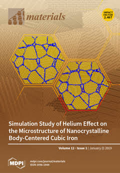
Chrunik, Maciej; Bubnov, Alexej; Minikayev, Roman; Lysak, Anastasiia; Włodarczyk, Damian; Nowicki, Marek; Chlanda, Adrian; Michalska-Domańska, Marta; Szczęśniak, Barbara; Gratzke, Mateusz
Influence of the Nd Dopant Content in Bi3TeBO9 Powders on Their Optical Nonlinearity Journal Article
In: Materials, vol. 18, pp. 5545, 2025.
@article{Mater_MN2026,

title = {Influence of the Nd Dopant Content in Bi3TeBO9 Powders on Their Optical Nonlinearity},

author = {Maciej Chrunik and Alexej Bubnov and Roman Minikayev and Anastasiia Lysak and Damian Włodarczyk and Marek Nowicki and Adrian Chlanda and Marta Michalska-Domańska and Barbara Szczęśniak and Mateusz Gratzke},

doi = {10.3390/ma18245545},

year  = {2025},

date = {2025-12-10},

journal = {Materials},

volume = {18},

pages = {5545},

abstract = {Second harmonic generation measurements for neodymium-doped bismuth–tellurium borate (Bi3TeBO9:Nd3+) powders are shown for the first time. Using undoped and low-content Nd3+-doped samples associated with the strongest nonlinear optical response, studies of temperature-dependent second-harmonic generation near the absorption edge were conducted. Spectroscopic measurements of the investigated powders revealed characteristic Nd3+ absorption bands and helped to estimate the corresponding energy band gaps for the chosen samples. The influence of low Nd3+-content on the absorption edge shift, as well as on the enhancement of second-harmonic generation and its temperature attenuation, is discussed. Temperature-dependent X-ray diffraction measurements enabled researchers to calculate the thermal expansion coefficients for undoped and Nd3+-doped Bi3TeBO9 and to assess the impact of this phenomenon on its acentricity. Thermogravimetric studies demonstrated the absence of phase transitions for the chosen samples up to their incongruent melting points. Energy Dispersive X-ray Spectroscopy measurements verified the uniformity of Nd3+ distribution in doped Bi3TeBO9 powders. The suitability of polycrystalline Bi3TeBO9:Nd3+ as media for the self-frequency doubling devices for potential optoelectronic and biomedical applications was assessed. The finest fractions of deagglomerated and suspended powders were extracted and demonstrated near-nanostructural morphology of separated particles, as revealed by means of atomic force microscopy.},

keywords = {},

pubstate = {published},

tppubtype = {article}

}
Przychodnia, Marta; Drechsler, Alina; Bazarnik, Maciej; Schlenhoff, Anika
STM/STS studies of single-atom Fe inclusions in MBE-grown monolayer MoS2/Gr/Ir(111) Conference
XIII Workshop on Applications of Scanning Probe Microscopy – STM/AFM 2025, Zakopane, 26 - 30 Listopada, 2025, (Oral presentation).
@conference{Zakopane25_MP,

title = {STM/STS studies of single-atom Fe inclusions in MBE-grown monolayer MoS2/Gr/Ir(111)},

author = {Marta Przychodnia and Alina Drechsler and Maciej Bazarnik and Anika Schlenhoff},

url = {https://nano.put.poznan.pl/wp-content/uploads/2025/12/zakopane2025_MP.pdf},

year  = {2025},

date = {2025-11-28},

urldate = {2025-11-28},

booktitle = {XIII Workshop on Applications of Scanning Probe Microscopy – STM/AFM 2025},

address = {Zakopane, 26 - 30 Listopada},

abstract = {Transition metal dichalcogenides (TMDs) have drawn significant attention due to their scalability and the thickness-dependence of their electronic density of states (DOS). Moreover, dimensionally confined TMDs, mainly 2D monolayers (MLs), are highly sensitive to structural defects, such as vacancies, interstitial and substituent atoms. Even in very low-density regimes, these impurities significantly affect various properties by introducing stress and/or modifying the DOS. Consequently, there are ongoing efforts to engineer defects in TMDs to tune their electronic, magnetic, optical, and catalytic properties. While most of the current research focuses on naturally occurring defects in chemical vapor deposited TMDs, to improve control over defect engineering, we focus on intentional single-atom inclusions in TMDs grown by molecular beam epitaxy (MBE).

In this presentation, I summarize our scanning tunneling microscopy (STM) and spectroscopy (STS) studies of Fe inclusions in ML MoS2 on Gr/Ir(111), which we realize by co-evaporating Fe during MoS2 MBE growth. We identify the Fe inclusions upon comparison with naturally occurring defects found on the undoped MoS2 grown previously in the same UHV chamber.  STS experiments reveal the presence of in-gap states arising from the incorporation of Fe atoms, whose spatial distributions are imaged by means of bias-dependent differential conductance mapping. Furthermore, resonant tunneling spectroscopy shows that the image potential states (IPS) are modified by the Fe inclusions, influencing the IPS’ energetic positions due to a variation in the local work function.


Funding from the Ministry of Science and Higher Education (Poland) within Project 0512/SBAD/2520.

},

note = {Oral presentation},

keywords = {},

pubstate = {published},

tppubtype = {conference}

}
In this presentation, I summarize our scanning tunneling microscopy (STM) and spectroscopy (STS) studies of Fe inclusions in ML MoS2 on Gr/Ir(111), which we realize by co-evaporating Fe during MoS2 MBE growth. We identify the Fe inclusions upon comparison with naturally occurring defects found on the undoped MoS2 grown previously in the same UHV chamber. STS experiments reveal the presence of in-gap states arising from the incorporation of Fe atoms, whose spatial distributions are imaged by means of bias-dependent differential conductance mapping. Furthermore, resonant tunneling spectroscopy shows that the image potential states (IPS) are modified by the Fe inclusions, influencing the IPS’ energetic positions due to a variation in the local work function.
Funding from the Ministry of Science and Higher Education (Poland) within Project 0512/SBAD/2520.
Kałuziak, Piotr; Kwiecień, Katarzyna; Raczyński, Jan; Nowicki, Marek; Majchrzycki, Łukasz; Szczęsny, Michał; Gawinkowski, Sylwester; Larowska-Zarych, Daria; El-Ahmar, Semir; Koczorowski, Wojciech
XIII Workshop on Applications of Scanning Probe Microscopy – STM/AFM 2025, Zakopane, 26 - 30 Listopada, 2025, (Oral presentation).
@conference{Zakopane25_PK,

title = {Surface Characterization of Thin-Layer Materials for Potential Applications in Physical Unclonable Functions},

author = {Piotr Kałuziak and Katarzyna Kwiecień and Jan Raczyński and Marek Nowicki and Łukasz Majchrzycki and Michał Szczęsny and Sylwester Gawinkowski and Daria Larowska-Zarych and Semir El-Ahmar and Wojciech Koczorowski},

url = {https://nano.put.poznan.pl/wp-content/uploads/2025/12/zakopane2025_PK.pdf},

year  = {2025},

date = {2025-11-28},

urldate = {2025-11-28},

booktitle = {XIII Workshop on Applications of Scanning Probe Microscopy – STM/AFM 2025},

address = {Zakopane, 26 - 30 Listopada},

abstract = {Two-dimensional (2D) materials and thin semiconductor films exhibit unique properties that make them attractive for applications in electronics, sensing, and information security. Here, we investigate selected layered systems to explore their potential for physical unclonable functions (PUFs), focusing on characteristic nanoscale features revealed by Raman spectroscopy, AFM, and SEM.

Continuous PtSe2films covered with gold nanoparticles were studied using surface-enhanced Raman spectroscopy (SERS), revealing enhanced vibrational signatures. Additionally, AFM measurements confirmed low roughness at the nanoscale morphology. Exfoliated ZrS2 flakes were analyzed by conventional Raman spectroscopy and AFM techniques, highlighting thickness variations and different degrees of surface oxidation properties that appear highly specific to the sample. Finally, chemically modified InSb layers examined with AFM and SEM showed surface roughness variations and etching-induced morphological changes. These results demonstrate that intrinsic disorder, film morphology, and surface modifications can generate unique and irreproducible features. The combined use of SERS, Raman spectroscopy, AFM, and SEM provides a comprehensive framework for evaluating the suitability of thin-layer materials as candidates for secure PUF schemes.


Funding from the Ministry of Science and Higher Education under project no. 0512/SBAD/6220.

Funding from the Ministry of Science and Higher Education under project no. 0512/SBAD/2520.},

note = {Oral presentation},

keywords = {},

pubstate = {published},

tppubtype = {conference}

}
Continuous PtSe2films covered with gold nanoparticles were studied using surface-enhanced Raman spectroscopy (SERS), revealing enhanced vibrational signatures. Additionally, AFM measurements confirmed low roughness at the nanoscale morphology. Exfoliated ZrS2 flakes were analyzed by conventional Raman spectroscopy and AFM techniques, highlighting thickness variations and different degrees of surface oxidation properties that appear highly specific to the sample. Finally, chemically modified InSb layers examined with AFM and SEM showed surface roughness variations and etching-induced morphological changes. These results demonstrate that intrinsic disorder, film morphology, and surface modifications can generate unique and irreproducible features. The combined use of SERS, Raman spectroscopy, AFM, and SEM provides a comprehensive framework for evaluating the suitability of thin-layer materials as candidates for secure PUF schemes.
Funding from the Ministry of Science and Higher Education under project no. 0512/SBAD/6220.
Funding from the Ministry of Science and Higher Education under project no. 0512/SBAD/2520.
Kwiecień, Katarzyna; Kałuziak, Piotr; Raczyński, Jan; Puchalska, Agnieszka; Dychalska, Anna; Chłopocka, Edyta; Kot, Dawid; Szybowicz, Mirosław; Jurczyszyn, Leszek; Dobrotvorska, Mariya V.; Lewandowski, Mikołaj; Koczorowski, Wojciech
Comparative analysis of group IV bulk TMDs' surface stability under ambient conditions Conference
XIII Workshop on Applications of Scanning Probe Microscopy – STM/AFM 2025, Zakopane, 26 - 30 Listopada, 2025, (Oral presentation).
@conference{Zakopane25_KK,

title = {Comparative analysis of group IV bulk TMDs' surface stability under ambient conditions},

author = {Katarzyna Kwiecień and Piotr Kałuziak and Jan Raczyński and Agnieszka Puchalska and Anna Dychalska and Edyta Chłopocka and Dawid Kot and Mirosław Szybowicz and Leszek Jurczyszyn and Mariya V. Dobrotvorska and Mikołaj Lewandowski and Wojciech Koczorowski},

url = {https://nano.put.poznan.pl/wp-content/uploads/2025/12/zakopane2025_KK.pdf},

year  = {2025},

date = {2025-11-27},

booktitle = {XIII Workshop on Applications of Scanning Probe Microscopy – STM/AFM 2025},

address = {Zakopane, 26 - 30 Listopada},

abstract = {Group IV Transition Metal Dichalcogenides (TMDs) possess attractive electronic properties, such as a tunable band gap in the 1-2 eV range and predicted charge carrier mobilities in the thousands of cm^2 V^-1 s^-1. Unlike most TMDs, they are not chemically inert under ambient conditions. Oxidation can alter their surface properties and morphology, making it essential to study the changes as they impact technological processing of group IV TMDs and their performance in electronic devices. In our earlier work, we demonstrated that HfSe2 undergoes rapid oxidation, resulting in Se-rich blister formation, oxygen diffusion into the bulk of the crystal, and HfO2 growth on the surface. In this study, we extend our investigation to HfS2 and ZrS2, comparing the impact of ambient air exposure on their surfaces with that observed for HfSe2. Scanning electron microscopy (SEM) reveals morphological differences: while HfSe2 shows bright blister-like features, sulfides develop areas with different charge carrier concentration that gradually rise in number with increasing exposure time to ambient air. Raman spectroscopy (RS) indicates that the vibrational modes of HfS2 and ZrS2 remain mostly unaffected, suggesting higher chemical stability compared to HfSe2, whose RS modes change drastically as the surface oxidation progresses. Complementary X-ray photoemission spectroscopy (XPS) data describes the influence of the ambient air exposure on the investigated materials' surface chemical deposition. These results provide a comprehensive picture of the morphological and chemical differences in group IV TMD oxidation, highlighting the role of chemical composition in determining their surface stability, which affects their integration potential with silicon-based electronics.


Funding from of Ministry of Science and Higher Education under project no. 0512/SBAD/6220.

Funding from of Ministry of Science and Higher Education under project no. 0512/SBAD/2520.},

note = {Oral presentation},

keywords = {},

pubstate = {published},

tppubtype = {conference}

}
Funding from of Ministry of Science and Higher Education under project no. 0512/SBAD/6220.
Funding from of Ministry of Science and Higher Education under project no. 0512/SBAD/2520.
Reddig, Wiktoria; Ciuk, Tymoteusz; Szary, Maciej J.; Jagiełło, Jakub; Dobrowolski, Artur; Prokopowicz, Rafał; Weiss, Marek; Wzorek, Marek; El-Ahmar, Semir
XIII Workshop on Applications of Scanning Probe Microscopy – STM/AFM 2025, Zakopane, 26 - 30 Listopada, 2025, (Oral presentation).
@conference{Zakopane25_WR,

title = {Radiation Resilience of Graphene Based Heterostructures Insights from Multimodal Structure Characterization},

author = {Wiktoria Reddig and Tymoteusz Ciuk and Maciej J. Szary and Jakub Jagiełło and Artur Dobrowolski and Rafał Prokopowicz and Marek Weiss and Marek Wzorek and Semir El-Ahmar},

url = {https://nano.put.poznan.pl/wp-content/uploads/2025/12/zakopane2025_WR.pdf},

year  = {2025},

date = {2025-11-27},

urldate = {2025-11-27},

booktitle = {XIII Workshop on Applications of Scanning Probe Microscopy – STM/AFM 2025},

address = {Zakopane, 26 - 30 Listopada},

abstract = {Enhancing the durability of magnetic field diagnostic electronics under fast-neutron irradiation requires materials capable of withstanding extreme defect formation. Dimensionality reduction offers a potential route, as two-dimensional systems inherently limit the development of collision cascades responsible for radiation damage in bulk materials. Graphene, with its two-dimensional nature and low neutron-collision cross section, embodies this concept. Yet, when integrated into a heterostructure, can

it maintain its intrinsic radiation resilience?

We explore the neutron radiation tolerance of an a-Al2O3/graphene/H-intercalated SiC(0001) heterostructure, combining reduced dimensionality with a conventional substrate platform. Using high-resolution transmission electron microscopy, Raman spectroscopy, electrical characterization and other techniques, we assess the material's structural and functional stability under fast-neutron fluences up to 2E18 n cm^-2 . Our findings show, the graphene layers exhibit negligible structural damage in comparison to bulk elements

Showing that graphene retains its structural integrity and electronic performance even under extreme neutron exposure, we suggest a viable route toward radiation-resilient sensor technologies. Such resilience is particularly crucial for future fusion energy systems, where long-term, reliable magnetic diagnostics will be key to successful reactor operation.


Funding from the Ministry of Science and Higher Education (Poland) for support under the project no. 0512/SBAD/2520.

Funding from the 'PhDBoost' Program for doctoral students of the Doctoral School of Poznan University of Technology (in 2024) from the University's subsidyfinancedfrom the funds of Ministry of Science and Higher Education.},

note = {Oral presentation},

keywords = {},

pubstate = {published},

tppubtype = {conference}

}
it maintain its intrinsic radiation resilience?
We explore the neutron radiation tolerance of an a-Al2O3/graphene/H-intercalated SiC(0001) heterostructure, combining reduced dimensionality with a conventional substrate platform. Using high-resolution transmission electron microscopy, Raman spectroscopy, electrical characterization and other techniques, we assess the material's structural and functional stability under fast-neutron fluences up to 2E18 n cm^-2 . Our findings show, the graphene layers exhibit negligible structural damage in comparison to bulk elements
Showing that graphene retains its structural integrity and electronic performance even under extreme neutron exposure, we suggest a viable route toward radiation-resilient sensor technologies. Such resilience is particularly crucial for future fusion energy systems, where long-term, reliable magnetic diagnostics will be key to successful reactor operation.
Funding from the Ministry of Science and Higher Education (Poland) for support under the project no. 0512/SBAD/2520.
Funding from the 'PhDBoost' Program for doctoral students of the Doctoral School of Poznan University of Technology (in 2024) from the University's subsidyfinancedfrom the funds of Ministry of Science and Higher Education.
Raczyński, Jan
Badanie właściwości fizycznych cienkowarstwowych interfejsów metal/PtSe2 PhD Thesis
2025, (Poznan University of Technology).
@phdthesis{RaczynskiPhD2025,

title = {Badanie właściwości fizycznych cienkowarstwowych interfejsów metal/PtSe2},

author = {Jan Raczyński},

url = {https://sin.put.poznan.pl/files/download/65282},

year  = {2025},

date = {2025-10-24},

urldate = {2025-10-24},

abstract = {The potential applications of two-dimensional materials, arising from their unique physicochemical properties, are being intensively studied. Current research focuses on characterizing these materials' properties and integrating them with existing CMOS technology, where interactions at metal / 2D-material interfaces play a crucial role. One of the most promising candidates for this technology is platinum diselenide (PtSe2), which, among others, exhibits high chemical stability and is expected to have high mobility of electric charge carriers. This doctoral dissertation focuses on the experimental analysis of the physical properties of PtSe2-based systems containing a specified number of monolayers deposited on an insulating substrate, as well as thin-film metal / PtSe2 interfaces. The selected metals (Ti, Cr, Ni, Pd, and Pt) used in these interfaces typically serve as buffer layers for electrodes in prototype electronic devices based on layered materials. Furthermore, a procedure for fabricating simple electronic devices using PtSe2 layers deposited on an Al2O3 substrate has been developed. The experimental work employed standard surface physics analysis techniques, including Raman spectroscopy, X-ray photoelectron spectroscopy, and microscopic techniques such as scanning electron microscopy and atomic force microscopy. The structuring process involved two steps of maskless optical lithography, followed by Ar+ plasma etching and DC magnetron metal deposition. The most significant results obtained in this dissertation include: I. Determination of Raman spectra for 1-10 ML PtSe2 / Al2O3 systems and their analysis in terms of thickness and quality compared to the bulk crystal. II. Characterization of chemical interactions and surface morphology for 10 and 15 [nm] thick metallic layers formed on the PtSe2 surface. III. Development and verification of the electron device structuring procedure using the TLM structure, which incorporates Ni (20 [nm]) / Au (40 [nm]) metal electrodes on a 3ML PtSe2 layer deposited on Al2O3. This doctoral thesis comprises seven chapters, including an introduction and a summary. The second chapter presents the properties of layered materials, with particular emphasis on PtSe2. The third chapter describes the preparation of the studied samples and the applied measurement methodology. The subsequent chapters present experimental results and their analysis: the fourth chapter discusses the PtSe2 / Al2O3 thin-film systems, the fifth chapter examines the physicochemical properties of the metal / PtSe2 interfaces, and the sixth chapter details the developed structuring method and Transfer Length Method (TLM) results for the structured 3 ML PtSe2 / Al2O3 system.},

note = {Poznan University of Technology},

keywords = {},

pubstate = {published},

tppubtype = {phdthesis}

}

El-Ahmar, Semir; Szary, Maciej J.; Reddig, Wiktoria; Jagiełło, Jakub; Dobrowolski, Artur; Ziemba, Maciej; Prokopowicz, Rafał; Ciuk, Tymoteusz
Grafen epitaksjalny w energetyce jądrowej: wyzwania i możliwości wsparte technikami próżniowymi Conference
IX Kongres Polskiego Towarzystwa Próżniowego, Poznań, 25-26 września, 2025, (Oral presentation).
@conference{PTP2025_SA,

title = {Grafen epitaksjalny w energetyce jądrowej: wyzwania i możliwości wsparte technikami próżniowymi},

author = {Semir El-Ahmar and Maciej J. Szary and Wiktoria Reddig and Jakub Jagiełło and Artur Dobrowolski and Maciej Ziemba and Rafał Prokopowicz and Tymoteusz Ciuk},

url = {https://nano.put.poznan.pl/wp-content/uploads/2025/09/PTP2025_SA.pdf},

year  = {2025},

date = {2025-09-26},

urldate = {2025-09-26},

booktitle = {IX Kongres Polskiego Towarzystwa Próżniowego},

address = {Poznań, 25-26 września},

abstract = {Dążenie do rozwoju reaktorów opartych na fuzji jądrowej wiąże się z koniecznością pogłębienia wiedzy na temat środowisk silnego promieniowania oraz pilnym opracowaniem technologii diagnostycznych odpornych na ekstremalne warunki radiacyjne. W miarę przesuwania granic technologicznych, materiały i układy pomiarowe wystawione są na działanie promieniowania o coraz większym natężeniu, co zbliża konwencjonalne rozwiązania do granic ich wytrzymałości. Wyzwanie to nabiera szczególnego znaczenia w kontekście praktycznej realizacji syntezy jądrowej jako źródła energii, gdzie niezawodne, odporne na promieniowanie czujniki – zwłaszcza magnetyczne – są kluczowe dla bezpiecznej i ciągłej kontroli procesów zachodzących wewnątrz reaktora. Nasze badania koncentrują się na eksploracji potencjału dwuwymiarowych (2D) struktur węglowych jako detektorów pola magnetycznego zdolnych do pracy w ekstremalnych warunkach środowiskowych, charakterystycznych dla przyszłych elektrowni termojądrowych. W tego typu reaktorach elektronika narażona będzie na wysokie temperatury oraz intensywne promieniowanie jonizujące, w tym neutronowe. Przedstawiamy wyniki eksperymentalnych badań dotyczących wpływu napromieniowania neutronowego na właściwości elektryczne układów opartych na grafenie epitaksjalnym. Wykorzystując min. metody próżniowe, wytworzyliśmy grafen quasi-swobodny z interkalacją wodorową na półizolacyjnych podłożach 4H-SiC(0001) i 6H-SiC(0001), pasywowanych warstwą Al2O3. Układy poddane zostały działaniu strumieni neutronów za pomocą badawczego reaktora jądrowego MARIA. Wśród kluczowych pytań pozostaje kwestia granicznej tolerancji na fluencję neutronów w systemach opartych na grafenie oraz to, czy ograniczona wymiarowość struktur 2D rzeczywiście zapewnia przewagę nad klasycznymi materiałami trójwymiarowymi. Szczególnie istotne jest także zrozumienie wpływu oddziaływań pomiędzy warstwami podłoża a warstwą grafenu w heterostrukturach 2D/3D, które mogą istotnie modyfikować — lub nawet ograniczać — korzyści wynikające z zastosowania architektury 2D. Odpowiedzi na te pytania są niezbędne do zaprojektowania nowej generacji elektroniki opartej na grafenie epitaksjalnym — zdolnej do niezawodnej pracy w warunkach intensywnego promieniowania, tam gdzie tradycyjne materiały i technologie mogą okazać się niewystarczające.


Funding from the Ministry of Science and Higher Education (Poland), Project No. 0512/SBAD/2520},

note = {Oral presentation},

keywords = {},

pubstate = {published},

tppubtype = {conference}

}
Funding from the Ministry of Science and Higher Education (Poland), Project No. 0512/SBAD/2520

Raczyński, Jan; Szczęsny, Michał; Koczorowski, Wojciech
PtSe2: From Layer to Device Conference
Workshop on Van der Waals Materials for Nanoelectronics, Poznan, September 1-2, 2025, (Invited lecture).
@conference{VdWM2025_JR,

title = {PtSe2: From Layer to Device},

author = {Jan Raczyński and Michał Szczęsny and Wojciech Koczorowski},

url = {https://nano.put.poznan.pl/wp-content/uploads/2025/10/WVWMN2025_JR.pdf},

year  = {2025},

date = {2025-09-02},

urldate = {2025-09-02},

booktitle = {Workshop on Van der Waals Materials for Nanoelectronics},

address = {Poznan, September 1-2},

abstract = {The growing interest in 2D materials in recent years has intensified research into understanding their physicochemical properties and related systems. Among the transition metal dichalcogenides

(TMDs) currently under intensive investigation is PtSe2, which exhibits a high theoretical value of charge carrier mobility and semiconducting properties in the single monolayer,

and high surface chemical stability. These features indicate significant potential for applications, including planar architecture devices based on PtSe2 layers. Furthermore, the energy

band gap in the TMD depends on various factors, such as the number of PtSe2 monolayers, strain in the system, structural defects and doping. The ability to band gap engineering,

combined with the formation of effective electrical contacts, calls for a comprehensive analysis of the physicochemical properties of both PtSe2 and metal/PtSe2 systems.

This presentation will discuss in detail the properties of the PtSe2/Al2O3 systems, in terms of the TMD material thickness, determined using nonpolarized and polarized Raman spectroscopy

(RS) measurements. Further discussion will focus on the influence of the deposited metal layer on the physicochemical properties of the metal/PtSe2 system using spectroscopic (RS and

XPS) and microscopic (SEM and AFM) techniques. These measurements will be presented both for the systems after metallic layer deposition and followed by thermal treatment at 500°C for

30 min. The discussion will conclude with the presentation of the 3L PtSe2-based transfer line measurement structure, fabricated using controlled argon plasma etching. The argon plasma

etching method, combined with the RS measurements, allows for the precise analysis of the PtSe2 layer degradation dynamics.


Funding from the National Science Centre (Poland) Project No. 2019/35/O/ST5/01940

Funding from the Ministry of Education and Science (Poland), Project No. 0512/SBAD/2520},

note = {Invited lecture},

keywords = {},

pubstate = {published},

tppubtype = {conference}

}
(TMDs) currently under intensive investigation is PtSe2, which exhibits a high theoretical value of charge carrier mobility and semiconducting properties in the single monolayer,
and high surface chemical stability. These features indicate significant potential for applications, including planar architecture devices based on PtSe2 layers. Furthermore, the energy
band gap in the TMD depends on various factors, such as the number of PtSe2 monolayers, strain in the system, structural defects and doping. The ability to band gap engineering,
combined with the formation of effective electrical contacts, calls for a comprehensive analysis of the physicochemical properties of both PtSe2 and metal/PtSe2 systems.
This presentation will discuss in detail the properties of the PtSe2/Al2O3 systems, in terms of the TMD material thickness, determined using nonpolarized and polarized Raman spectroscopy
(RS) measurements. Further discussion will focus on the influence of the deposited metal layer on the physicochemical properties of the metal/PtSe2 system using spectroscopic (RS and
XPS) and microscopic (SEM and AFM) techniques. These measurements will be presented both for the systems after metallic layer deposition and followed by thermal treatment at 500°C for
30 min. The discussion will conclude with the presentation of the 3L PtSe2-based transfer line measurement structure, fabricated using controlled argon plasma etching. The argon plasma
etching method, combined with the RS measurements, allows for the precise analysis of the PtSe2 layer degradation dynamics.
Funding from the National Science Centre (Poland) Project No. 2019/35/O/ST5/01940
Funding from the Ministry of Education and Science (Poland), Project No. 0512/SBAD/2520
Shuryhin, Fedir; Biliak, Roman; Liakh-Kaguy, Natalia; Kost, Yaroslav; Sukhorebryi, Serhii; Ciuk, Tymoteusz; El-Ahmar, Semir
Investigation of graphene-metal contacts in Hall sensors based on QFS graphene Journal Article
In: Molecular Crystals and Liquid Crystals, vol. 769, iss. 15-18, pp. 1538-1546, 2025.
@article{nokey,

title = {Investigation of graphene-metal contacts in Hall sensors based on QFS graphene},

author = {Fedir Shuryhin and Roman Biliak and Natalia Liakh-Kaguy and Yaroslav Kost and Serhii Sukhorebryi and Tymoteusz Ciuk and Semir El-Ahmar

},

doi = {10.1080/15421406.2025.2540100},

year  = {2025},

date = {2025-08-06},

urldate = {2025-08-06},

journal = {Molecular Crystals and Liquid Crystals},

volume = {769},

issue = {15-18},

pages = {1538-1546},

abstract = {This article presents a study of the current-voltage characteristics of metal–graphene contacts in Hall sensors based on quasi-free-standing graphene (QFS graphene) grown on 4H-SiC with hydrogen intercalation. Various graphene-based Hall sensor designs are reviewed. The study focuses on the linearity of the I–V characteristics in the contact regions. Sensors with titanium–gold contacts and Al2O3 passivation were fabricated. Results show highly ohmic behavior and strong agreement with a linear model, indicating high contact quality. The findings highlight the potential of QFS-graphene Hall sensors for high-sensitivity, stable applications and form a basis for future studies.},

keywords = {},

pubstate = {published},

tppubtype = {article}

}
Szary, Maciej J.; El-Ahmar, Semir; Prokopowicz, Rafał; Ciuk, Tymoteusz
Reduced dimensionality, elevated tolerance? A perspective on 2D materials for fusion diagnostics Journal Article
In: Journal of Physics: Condensed Matter, vol. 37, pp. 321501, 2025.
@article{MS_IOP_2025,

title = {Reduced dimensionality, elevated tolerance? A perspective on 2D materials for fusion diagnostics},

author = {Maciej J. Szary and Semir El-Ahmar and Rafał Prokopowicz and Tymoteusz Ciuk},

doi = {10.1088/1361-648X/adf481},

year  = {2025},

date = {2025-08-06},

journal = {Journal of Physics: Condensed Matter},

volume = {37},

pages = {321501},

abstract = {Whether in the distant reaches of outer space or deep within magnetic confinement fusion reactors, our exploration of high-energy particle radiation environments continues to evolve—driving an urgent need for diagnostic technologies capable of withstanding extreme radiation exposure. As these technological frontiers expand, materials are increasingly subjected to radiation intensities far beyond those encountered in previous decades, pushing conventional systems to their operational limits. This challenge is especially acute in the pursuit of practical fusion energy, where the development of resilient magnetic sensor technologies capable of sustained, reliable operation under intense neutron flux is essential. In this Perspective, we examine this challenge through the lens of condensed matter physics, proposing that reducing the dimensionality of sensing materials—from bulk to two-dimensional (2D) systems—offers a promising route to mitigate radiation-induced degradation. Lower dimensionality suppresses the formation of collision cascades, which are responsible for rapid defect accumulation in bulk materials, thereby offering a pathway toward radiation-tolerant sensor platforms. We focus on recent advances in graphene-based Hall sensors deployed in fast-neutron-radiation environments, where fluence levels up to 2 n cm−2 have been sustained with negligible structural damage, corresponding to a relative defect concentration below 0.01%. These findings underscore graphene’s potential as a candidate for neutron-radiation-resistant electronics. However, key open questions remain—most notably, the ultimate neutron fluence tolerance of graphene-based systems and the extent to which reduced dimensionality confers a measurable advantage over traditional three-dimensional (3D) materials. Additionally, we discuss the critical influence of substrate interactions in 2D/3D heterostructures, which may offset or complicate the benefits of 2D architectures. By addressing these challenges and identifying future directions, this article outlines a roadmap toward the development of graphene-based electronics capable of surviving—and performing—in the most extreme radiation environments, where conventional materials are prone to failure and low-dimensional systems may thrive.


Funding from the Ministry of Education and Science (Poland), Project No. 0512/SBAD/2520},

keywords = {},

pubstate = {published},

tppubtype = {article}

}
Funding from the Ministry of Education and Science (Poland), Project No. 0512/SBAD/2520
Kałużny, Jarosław; Pielecha, Ireneusz; Błaszkiewicz, Paulina; Boncel, Sławomir; Marek, Adam; Terzyk, Artur P.; Korczeniewski, Emil; Runka, Tomasz; Nowicki, Marek; Giedrowicz, Marcin
Carbon nanotubes as biofuel additives enabling advanced combustion modulation strategies Journal Article
In: Carbon, vol. 244, pp. 120686, 2025.
@article{JK_Carb_2025,

title = {Carbon nanotubes as biofuel additives enabling advanced combustion modulation strategies},

author = {Jarosław Kałużny and Ireneusz Pielecha and Paulina Błaszkiewicz and Sławomir Boncel and Adam Marek and Artur P. Terzyk and Emil Korczeniewski and Tomasz Runka and Marek Nowicki and Marcin Giedrowicz},

doi = {10.1016/j.carbon.2025.120686},

year  = {2025},

date = {2025-08-04},

journal = {Carbon},

volume = {244},

pages = {120686},

abstract = {This study investigates the effect of carbon nanotubes (CNTs) as ethanol fuel additives in a new class of bionanofuels for internal combustion and jet engines. In-cylinder pressure and thermodynamic behavior, including the heat release rate (HRR), were analyzed using a rapid compression machine (RCM) for pure ethanol, ethanol enriched with CNTs (2.5 mg/L), ethanol containing spherical gold nanoparticles (AuNPs, 0.01 g/L), and gasoline. CNT-enriched ethanol reduced maximum in-cylinder pressure by up to 13 % compared to pure ethanol and lowered the peak HRR by up to 43 % at low injection doses. The flame brightness, quantified by high-speed imaging, was reduced by over 50 %, indicating suppressed soot formation. AuNPs exhibited an opposite trend: after a short ignition delay, they increased HRR by up to 28 %, attributed to catalytic activity. CNTs, in contrast, acted via physical thermal dissipation, i.e., cooling of hot-spots through axial conductivity, and scavenging reactive free-radicals. Optical analysis also showed a smaller flame area and slower propagation speed for CNT fuels. These findings highlight the dual benefit of CNTs: enabling smoother combustion with reduced NOx and particulate precursors, and oxidizing cleanly in-cylinder, offering a scalable, environmentally favorable approach to combustion control in next-generation bionanofuels.},

keywords = {},

pubstate = {published},

tppubtype = {article}

}

Reddig, Wiktoria; El-Ahmar, Semir; Prokopowicz, Rafał; Ciuk, Tymoteusz
In the heart of the reactor: testing graphene for neutron-resilient electronics Conference
The PhD Science Forum Innovative thinking. Real data. Future science., Poznan, June, 27, 2025, (Poster presentation).
@conference{PhD_SF2025_WR,

title = {In the heart of the reactor: testing graphene for neutron-resilient electronics},

author = {Wiktoria Reddig and Semir El-Ahmar and Rafał Prokopowicz and Tymoteusz Ciuk},

url = {https://nano.put.poznan.pl/wp-content/uploads/2025/07/PhD_SF2025_WR.pdf},

year  = {2025},

date = {2025-06-27},

booktitle = {The PhD Science Forum Innovative thinking. Real data. Future science.},

address = {Poznan, June, 27},

abstract = {As the urgency of climate change accelerates, nuclear fusion emerges as a promising long-term energy solution. Among fusion technologies, magnetic confinement systems like tokamaks rely heavily on accurate magnetic field diagnostics. This work explores the development of Hall effect graphene-based magnetic sensors designed to operate in the extreme conditions found inside fusion reactors.

The research focuses on the performance of graphene-based sensors exposed to high temperatures and neutron radiation—two key stressors in fusion environments. To fabricate the sensors, hydrogenintercalated quasi-free-standing (QFS) graphene was grown on semi-insulating 4H-SiC(0001) and 6HSiC(0001) substrates and then coated with a protective Al2O3 layer. Neutron irradiation experiments were carried out at the MARIA reactor, operated by the Polish National Center for Nuclear Research, while thermal effects were evaluated in a separate study [5]. Measurements using the Hall effect, micro-Raman spectroscopy, and density functional theory indicate that the primary cause of performance degradation after irradiation is the loss of hydrogen from the intercalated

layer. This hydrogen depletion disrupts the unique electronic properties of QFS graphene. However, the research also shows that thermal annealing above 200◦C can partially reverse this damage—likely through hydrogen diffusion at elevated temperatures. The effectiveness of recovery depends on how much hydrogen was lost during irradiation [4]. Understanding these degradation and recovery mechanisms is essential for assessing the long-term viability of graphene-based sensors for magnetic diagnostics in fusion reactors and

other high-radiation environments


Funding from the Ministry of Science and Higher Education (Poland), Project No. 0512/SPHD/2501},

note = {Poster presentation},

keywords = {},

pubstate = {published},

tppubtype = {conference}

}
The research focuses on the performance of graphene-based sensors exposed to high temperatures and neutron radiation—two key stressors in fusion environments. To fabricate the sensors, hydrogenintercalated quasi-free-standing (QFS) graphene was grown on semi-insulating 4H-SiC(0001) and 6HSiC(0001) substrates and then coated with a protective Al2O3 layer. Neutron irradiation experiments were carried out at the MARIA reactor, operated by the Polish National Center for Nuclear Research, while thermal effects were evaluated in a separate study [5]. Measurements using the Hall effect, micro-Raman spectroscopy, and density functional theory indicate that the primary cause of performance degradation after irradiation is the loss of hydrogen from the intercalated
layer. This hydrogen depletion disrupts the unique electronic properties of QFS graphene. However, the research also shows that thermal annealing above 200◦C can partially reverse this damage—likely through hydrogen diffusion at elevated temperatures. The effectiveness of recovery depends on how much hydrogen was lost during irradiation [4]. Understanding these degradation and recovery mechanisms is essential for assessing the long-term viability of graphene-based sensors for magnetic diagnostics in fusion reactors and
other high-radiation environments
Funding from the Ministry of Science and Higher Education (Poland), Project No. 0512/SPHD/2501

Jagiełło, Jakub; Dobrowolski, Artur; Ciuk, Tymoteusz; Prokopowicz, Rafał; Bieńkowska, Barbara; Włodarczyk, Jakub; El-Ahmar, Semir; Szary, Maciej J.; Szybowicz, Mirosław
In: Results in Physics, vol. 75, pp. 108332, 2025.
@article{JJ_RiP_2025,

title = {Dosimetric platform and a genuine Raman protocol for passive estimation of fast-neutron fluence in irradiated SiC and SiC topped with epitaxial graphene},

author = {Jakub Jagiełło and Artur Dobrowolski and Tymoteusz Ciuk and Rafał Prokopowicz and Barbara Bieńkowska and Jakub Włodarczyk and Semir El-Ahmar and Maciej J. Szary and Mirosław Szybowicz},

doi = {10.1016/j.rinp.2025.108332},

year  = {2025},

date = {2025-06-27},

journal = {Results in Physics},

volume = {75},

pages = {108332},

abstract = {The article introduces a genuine ex-situ measurement protocol to estimate the integrated flux of mostly fast (1-2 MeV) neutrons. It is verified up to the fluence of 6.5 × 10¹⁸ n/cm2. A dedicated dosimetric platform comprises p-type hydrogen-intercalated quasi-free-standing epitaxial Chemical Vapor Deposition graphene on semi-insulating vanadium-compensated nominally on-axis 6H-SiC(0001) and a 100-nm-thick atomic-layerdeposited amorphous aluminum oxide encapsulation. The methodology correlates the total area under the averaged Raman spectra of SiC, between 60 cm-1 and 1200 cm-1, upon prior normalization to the maximum value of the longitudinal optical mode at 964 cm-1. The patterned a-Al2O3/QFS-graphene/6H-SiC(0001) system offers two verification mechanisms — one within the graphene mesa and the other outside. Following the protocol, one can read the neutron fingerprint in the material and relate it to the integrated flux. The passive character of the method eliminates the radiological hazards associated with traditional activation methods. The approach enables localized and precise fluence control in fissile and thermonuclear facilities with a Root Mean Squared Percentage Error of the fitted model of approximately 4%.


Funding from the Ministry of Education and Science (Poland), Project No. 0512/SBAD/2520 and Project No. 0512/SBAD/2551},

keywords = {},

pubstate = {published},

tppubtype = {article}

}
Funding from the Ministry of Education and Science (Poland), Project No. 0512/SBAD/2520 and Project No. 0512/SBAD/2551
Reddig, Wiktoria; Ciuk, Tymoteusz; Prokopowicz, Rafał; El-Ahmar, Semir
The impact of neutron radiation and high temperatures on graphene-based magnetic field sensors Conference
European Nuclear Young Generation Forum 2025, Zagreb, June, 2-6, 2025, (Oral presentation ).
@conference{ENYGF_2025,

title = {The impact of neutron radiation and high temperatures on graphene-based magnetic field sensors},

author = {Wiktoria Reddig and Tymoteusz Ciuk and Rafał Prokopowicz and Semir El-Ahmar},

url = {https://nano.put.poznan.pl/wp-content/uploads/2025/07/ENYGF-25-Paper_Reddig_rev2.pdf},

year  = {2025},

date = {2025-06-02},

urldate = {2025-06-02},

booktitle = {European Nuclear Young Generation Forum 2025},

address = {Zagreb, June, 2-6},

abstract = {This paper presents new findings on the electrical characterisation of epitaxial graphene-based radiation-resistant magnetic field sensors following exposure to a neutron fluence of 4.0 × 10^18 n/cm² — twice the highest fluence previously examined. The collected results have been framed in the context of existing research. Additionally, the paper outlines future research directions aimed at further investigating the performance of these sensors under varying radiation conditions and exploring ways to enhance their resilience for practical applications.


Funding from the Ministry of Science and Higher Education (Poland), Project No. 0512/SBAD/2520 and 0512/SPHD/2501},

note = {Oral presentation

},

keywords = {},

pubstate = {published},

tppubtype = {conference}

}
Funding from the Ministry of Science and Higher Education (Poland), Project No. 0512/SBAD/2520 and 0512/SPHD/2501
Leśniewski, Bartosz; Kopani, Martin; Szczurek, Anna; Matczak, Michał; Dubowik, Janusz; Kotula, Martyna; Kubiak, Anita; Tsurkan, Dmitry; Romańczuk-Ruszyk, Eliza; Nowicki, Marek; Nowacki, Krzysztof; Petrenko, Iaroslav; Ehrlich, Hermann
Development of Magnetic Sponges Using Steel Melting on 3D Carbonized Spongin Scaffolds Under Extreme Biomimetics Conditions Journal Article
In: Biomimetics, vol. 10, iss. 6, pp. 350, 2025.
@article{Nowicki_Biomim_2025,

title = {Development of Magnetic Sponges Using Steel Melting on 3D Carbonized Spongin Scaffolds Under Extreme Biomimetics Conditions},

author = {Bartosz Leśniewski and Martin Kopani and Anna Szczurek and Michał Matczak and Janusz Dubowik and Martyna Kotula and Anita Kubiak and Dmitry Tsurkan and Eliza Romańczuk-Ruszyk and Marek Nowicki and Krzysztof Nowacki and Iaroslav Petrenko and Hermann Ehrlich},

doi = {10.3390/biomimetics10060350},

year  = {2025},

date = {2025-05-28},

journal = {Biomimetics},

volume = {10},

issue = {6},

pages = {350},

abstract = {This study presents a novel approach to fabricating magnetic sponge-like composites by melting various types of steel onto three-dimensional (3D) carbonized spongin scaffolds under extreme biomimetic conditions. Spongin, a renewable marine biopolymer with high thermal stability, was carbonized at 1200 °C to form a turbostratic graphite matrix capable of withstanding the high-temperature steel melting process (1450–1600 °C). The interaction between molten steel vapors and the carbonized scaffolds resulted in the formation of nanostructured iron oxide (primarily hematite) coatings, which impart magnetic properties to the resulting composites. Detailed characterization using SEM-EDX, HRTEM, FT-IR, and XRD confirmed the homogeneous distribution of iron oxides on and within the carbonized fibrous matrix. Electrochemical measurements further demonstrated the electrocatalytic potential of the composite, particularly the sample modified with stainless steel 316L—for the hydrogen evolution reaction (HER), offering promising perspectives for green hydrogen production. This work highlights the potential of extreme biomimetics to create functional, scalable, and sustainable materials for applications in catalysis, environmental remediation, and energy technologies.


Funding from theMinistry of Science and Higher Education, (Poland), Project No. 0911/SBAD/2502},

keywords = {},

pubstate = {published},

tppubtype = {article}

}
Funding from theMinistry of Science and Higher Education, (Poland), Project No. 0911/SBAD/2502
Przychodnia, Marta; Bazarnik, Maciej
Ferromagnetism in Two-Dimensional Dysprosium−Platinum Surface Alloy Journal Article
In: Nano Letters, vol. 25, iss. 24, pp. 9519, 2025.
@article{Przychodnia_NL_2025,

title = {Ferromagnetism in Two-Dimensional Dysprosium−Platinum Surface Alloy},

author = {Marta Przychodnia and Maciej Bazarnik},

doi = {10.1021/acs.nanolett.5c00262},

year  = {2025},

date = {2025-05-17},

urldate = {2025-05-17},

journal = {Nano Letters},

volume = {25},

issue = {24},

pages = {9519},

abstract = {In this study, we comprehensively analyze single and triplelayers of a new two-dimensional surface alloy, namely DyPt2. Both areferromagnetic materials with an in-plane easy magnetization axis and lowCurie temperature on the order of a few Kelvins. Magnetic and electronicproperties confirm weak interlayer coupling and the dominance ofinteractions within alloy layers. Atomic-scale investigation proved nearlythe same atomic structure of the termination layer and varying moirépatterns. The electronic structures of single and triple layer DyPt2 are similar,consisting of a mixture of Dy and Pt electronic states. The intensity of theseelectronic states varies within the moiré pattern, similar to the surface localwork function, demonstrating modulated coupling between the surface alloyand the substrate. The presented results provide essential knowledge for further research of this system in terms of its application inthe growth of densely packed arrays of magnetic clusters and molecules.


Funding from the Ministry of Education and Science (Poland), Project No. 0512/SBAD/2520

Funding from the National Science Centre (Poland) Project No. 2019/33/N/ST5/01711 },

keywords = {},

pubstate = {published},

tppubtype = {article}

}
Funding from the Ministry of Education and Science (Poland), Project No. 0512/SBAD/2520
Funding from the National Science Centre (Poland) Project No. 2019/33/N/ST5/01711

El-Ahmar, Semir; Szary, Maciej J.; Reddig, Wiktoria; Jagiełło, Jakub; Prokopowicz, Rafał; Ziemba, Maciej; Dobrowolski, Artur; Ciuk, Tymoteusz
Epitaxial graphene technology for the future nuclear industry Conference
Workshop on Bulk Crystal Growth and Epitaxy (WBCGE), Warsaw, May 15-16, 2025, (Invited lecture).
@conference{WBCGE2025_SA,

title = {Epitaxial graphene technology for the future nuclear industry},

author = {Semir El-Ahmar and Maciej J. Szary and Wiktoria Reddig and Jakub Jagiełło and Rafał Prokopowicz and Maciej Ziemba and Artur Dobrowolski and Tymoteusz Ciuk},

url = {https://nano.put.poznan.pl/wp-content/uploads/2025/05/WBCGE2025_SA.pdf},

year  = {2025},

date = {2025-05-16},

urldate = {2025-05-16},

booktitle = {Workshop on Bulk Crystal Growth and Epitaxy (WBCGE)},

address = {Warsaw, May 15-16},

abstract = {In the development of magnetically confined fusion reactor technologies, our understanding of high-energy particle radiation environments is continually advancing. This creates an urgent need for diagnostic technologies that can endure extreme radiation exposure. As these technological boundaries expand, materials face radiation intensities that far exceed those encountered in previous decades, pushing conventional systems to their operational limits. This challenge is especially critical in the pursuit of practical fusion energy, where the creation of robust magnetic sensor technologies capable of continuous and reliable operation under intense neutron flux is essential. Our research explores the potential of using two-dimensional (2D) carbon structures as magnetic field detectors capable of operating in the extreme conditions of future thermonuclear power plants. In such reactors, electronics will be exposed to high temperatures and radiation damage. We demonstrate the experimental study on the impact of neutron radiation and determine its influence on the electrical parameters of epitaxial graphene-based systems. We have conducted preliminary research to investigate the impact of high temperature and neutron radiation. For this purpose, we fabricated a hydrogen-intercalated quasi-free-standing graphene on semi-insulating 4H-SiC(0001) and 6H SiC(0001), passivated with an Al2O3 layer. The systems were exposed to neutron fluxes using the MARIA research nuclear reactor. Key open questions include the ultimate neutron fluence tolerance of graphene-based systems and whether the reduced dimensionality offers a significant advantage over traditional 3D materials. Additionally, it's crucial to consider the impact of substrate interactions in 2D/3D heterostructures, as these can undermine or complicate the benefits of 2D architectures. By addressing these challenges and identifying future directions, we can develop a roadmap for epitaxial graphene-based electronics that can withstand and operate reliably in extreme radiation environments, where conventional materials are likely to fail.


Funding from the Ministry of Education and Science (Poland), Project No. 0512/SBAD/2520},

note = {Invited lecture},

keywords = {},

pubstate = {published},

tppubtype = {conference}

}
Funding from the Ministry of Education and Science (Poland), Project No. 0512/SBAD/2520
Szawioła, Gustaw; Mieloch, Szymon; Stefańska, Danuta; Głowacki, Przemysław; Frajtak, Agata; Michalczyk, Jędrzej; Murawski, Krzysztof; Pruchlat, Andrzej; Raczyński, Jan; Schmidt, Michał; Sobkowski, Jerzy; Wosicki, Maksymilian; Biadasz, Andrzej; Buczek, Adam; Dychalska, Anna; Mazarewicz, Piotr; Szybowicz, Mirosław
Thermal Effects in Optically Detected Magnetic Resonance of Nitrogen Vacancies in Diamond: A Quantum Thermometer for a Graduate Teaching Lab Journal Article
In: Journal of Chemical Education, vol. 102, iss. 5, pp. 1949-1959, 2025.
@article{GS_2025,

title = {Thermal Effects in Optically Detected Magnetic Resonance of Nitrogen Vacancies in Diamond: A Quantum Thermometer for a Graduate Teaching Lab},

author = {Gustaw Szawioła and Szymon Mieloch and Danuta Stefańska and Przemysław Głowacki and Agata Frajtak and Jędrzej Michalczyk and Krzysztof Murawski and Andrzej Pruchlat and Jan Raczyński and Michał Schmidt and Jerzy Sobkowski and Maksymilian Wosicki and Andrzej Biadasz and Adam Buczek and Anna Dychalska and Piotr Mazarewicz and Mirosław Szybowicz},

doi = {10.1021/acs.jchemed.4c01434},

year  = {2025},

date = {2025-04-17},

urldate = {2025-04-17},

journal = { Journal of Chemical Education},

volume = {102},

issue = {5},

pages = {1949-1959},

abstract = {This work reports a study of thermal effects in nitrogen vacancies in diamond using the optically detected continuous wave magnetic resonance (cw-ODMR) method. Changes in the ODMR signal induced by heating the diamond sample with both laser light at various powers and by a simple heater were investigated and analyzed. The influence of heating on the ODMR signal was measured for two types of synthetic diamond powder─a low cost microcrystalline powder (particle diameters ca. 80 μm) and a high purity nanodiamond powder (particle diameters ca. 140 nm). The experimental setup can be viewed as a pedagogical quantum thermometer. A number of cost-effective components were used, e.g., a self-constructed confocal microscope, and the Raspberry Pi 4B microcomputer in an experiment control and data acquisition system, as well as an inexpensive microwave modulator, analog to digital converter, and a heating plate.},

keywords = {},

pubstate = {published},

tppubtype = {article}

}
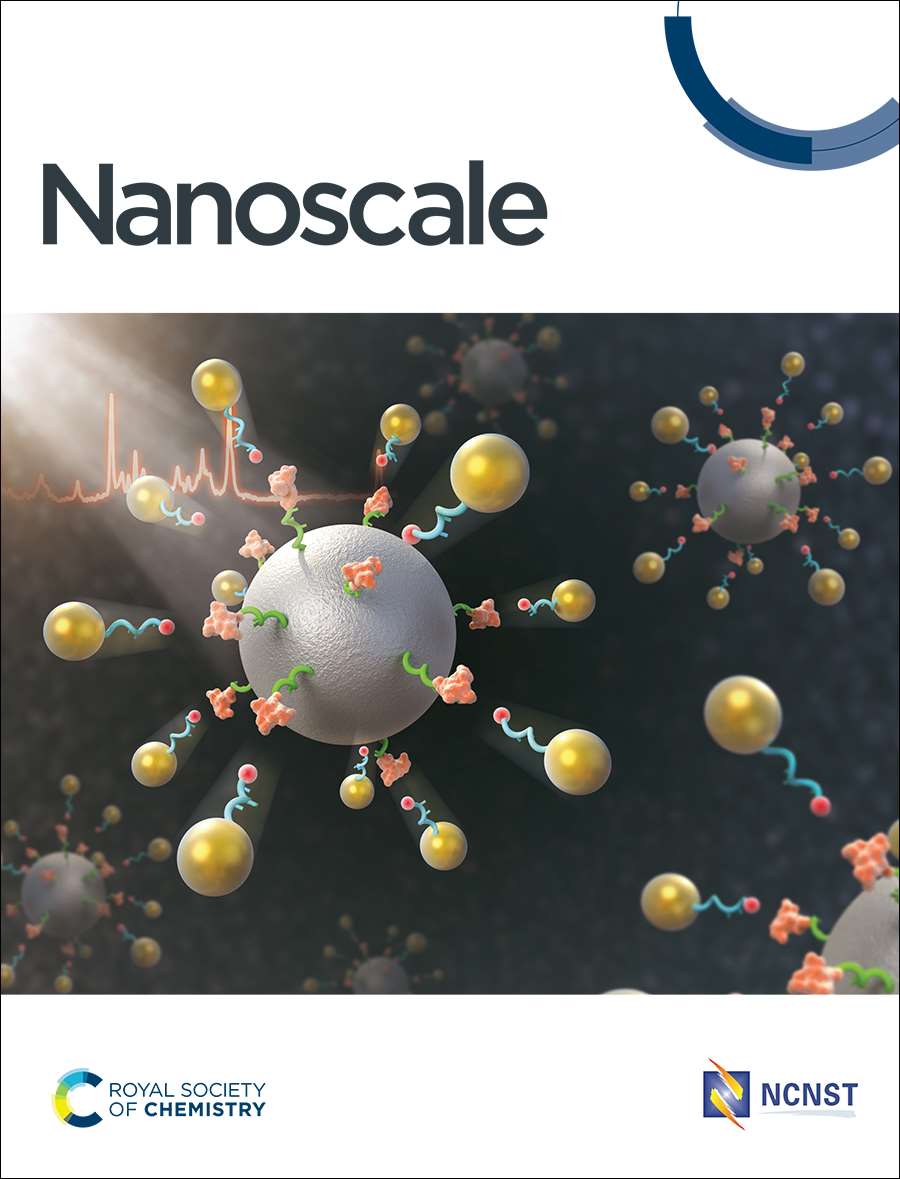
Raczyński, Jan; Nowaczyk, Jakub; Nowak, Ewelina; El-Ahmar, Semir; Chłopocka, Edyta; Szybowicz, Mirosław; Koczorowski, Wojciech
Thermally induced correlation effects studied by Raman spectroscopy in PtSe2/Al2O3 systems Journal Article
In: Nanoscale, vol. 17, iss. 20, pp. 12810, 2025.
@article{Raczynski_Nanoscale_2025,

title = {Thermally induced correlation effects studied by Raman spectroscopy in PtSe2/Al2O3 systems},

author = {Jan Raczyński and Jakub Nowaczyk and Ewelina Nowak and Semir El-Ahmar and Edyta Chłopocka and Mirosław Szybowicz and Wojciech Koczorowski},

doi = {10.1039/d4nr04062g},

year  = {2025},

date = {2025-04-15},

urldate = {2025-04-15},

journal = {Nanoscale},

volume = {17},

issue = {20},

pages = {12810},

abstract = {In this paper, we report the analysis of the Raman spectroscopy results of PtSe2 layers (ranging from 1 to 10 layers) deposited on an Al2O3 substrate, compared to those of the sub-micron thin flake and bulk PtSe2. The positions of typical PtSe2 Raman modes and the integral intensity ratios of the A1g and E1g bands are compared and discussed for all the systems considered in the temperature range from room temperature to 520 K. Moreover, the correlation plot of E1g and A1g is used to analyse the correlations of the dominant Raman modes in the PtSe2/Al2O3 systems, in which the frequency position (in-plane to out-of-plane) ratio exhibits a well-defined linear dependence on temperature.


Funding from the National Science Centre (Poland) Project No. 2019/35/O/ST5/01940},

keywords = {},

pubstate = {published},

tppubtype = {article}

}
Funding from the National Science Centre (Poland) Project No. 2019/35/O/ST5/01940
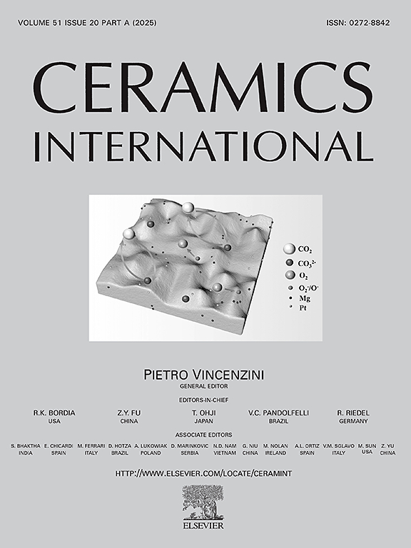
Chłopocka, Edyta; Szybowicz, Mirosław; Szafraniak-Wiza, Izabela; Stachowiak, Alicja; Koczorowski, Wojciech; Robakowska, Mariola
The influence of synthesis method on LaFeO3 and LaMnO3 powder properties Journal Article
In: Ceramics International, vol. 51, iss. 18, pp. 25552-25559, 2025.
@article{CeramWK_2025,

title = {The influence of synthesis method on LaFeO3 and LaMnO3 powder properties},

author = {Edyta Chłopocka and Mirosław Szybowicz and Izabela Szafraniak-Wiza and Alicja Stachowiak and Wojciech Koczorowski and Mariola Robakowska},

doi = {10.1016/j.ceramint.2025.03.237},

year  = {2025},

date = {2025-03-18},

journal = {Ceramics International},

volume = {51},

issue = {18},

pages = {25552-25559},

abstract = {Recently, searching for a lead-free inorganic alternative to organic-inorganic perovskite materials has been one of the main scientific issues in photovoltaics. Proposed LaMnO3 and LaFeO3 are narrow-band Mott insulators with a perovskite-like structure. In this work, the structural analysis of powders prepared by two different methods, i.e. sol-gel and mechanochemical synthesis, has been carried out. The characteristic temperatures in the sol-gel process have been determined using thermogravimetric analysis. The morphology of powders was observed with a scanning electron microscope. X-ray diffraction analysis enabled phase identification and subsequent determination of unit cell parameters using Rietveld refinement. Two complementary methods, Raman and Fourier-transform infrared spectroscopies, have been used to assess the structural differences between the samples. The obtained results suggest a significant influence of the synthesis method on the final powders’ properties.},

keywords = {},

pubstate = {published},

tppubtype = {article}

}
Kwiecień, Katarzyna; Raczyński, Jan; Puchalska, Agnieszka; Nowak, Ewelina; Chłopocka, Edyta; Kot, Dawid; Szybowicz, Mirosław; Jurczyszyn, Leszek; Koczorowski, Wojciech
The effects of short-term air exposure of the monocrystal HfSe2 surface Journal Article
In: Applied Surface Science, vol. 690, pp. 162546, 2025.
@article{Kwiecien_APSUSC_2025,

title = {The effects of short-term air exposure of the monocrystal HfSe2 surface},

author = {Katarzyna Kwiecień and Jan Raczyński and Agnieszka Puchalska and Ewelina Nowak and Edyta Chłopocka and Dawid Kot and Mirosław Szybowicz and Leszek Jurczyszyn and Wojciech Koczorowski},

doi = {10.1016/j.apsusc.2025.162546},

year  = {2025},

date = {2025-02-01},

urldate = {2025-02-01},

journal = {Applied Surface Science},

volume = {690},

pages = {162546},

abstract = {We report the impact of short-term sequential exposure to air–atmosphere conditions on the mechanically exfoliated surface of HfSe2 monocrystal. Our scanning electron microscopy studies show the early surface

oxidation dynamics with a rapid increase of the Se-rich blister coverage. Further X-ray photoemission and energy dispersive spectroscopy measurements reveal a progressive diffusion of O atoms into the bulk and

HfO2 layer formation on the surface during the exposure time. Finally, Raman spectroscopy measurements confirm the coexistence of HfSe2 and HfO2 on the surface. However, the Raman spectroscopy technique does

not allow quantitative determination of the degree of short-term surface oxidation. Additionally, we confirm the conclusions drawn from the experimental results with the results of the density functional theory calculations

of the O/HfSe2 adsorption system. The presented results hold substantial technological significance from the point of view of the application of HfSe2 in electronics by filling the gap in the early oxidation dynamics under ambient conditions.


Funding from the Ministry of Education and Science (Poland), Project No. 0512/SBAD/2420 and 0612/SBAD/6215},

keywords = {},

pubstate = {published},

tppubtype = {article}

}
oxidation dynamics with a rapid increase of the Se-rich blister coverage. Further X-ray photoemission and energy dispersive spectroscopy measurements reveal a progressive diffusion of O atoms into the bulk and
HfO2 layer formation on the surface during the exposure time. Finally, Raman spectroscopy measurements confirm the coexistence of HfSe2 and HfO2 on the surface. However, the Raman spectroscopy technique does
not allow quantitative determination of the degree of short-term surface oxidation. Additionally, we confirm the conclusions drawn from the experimental results with the results of the density functional theory calculations
of the O/HfSe2 adsorption system. The presented results hold substantial technological significance from the point of view of the application of HfSe2 in electronics by filling the gap in the early oxidation dynamics under ambient conditions.
Funding from the Ministry of Education and Science (Poland), Project No. 0512/SBAD/2420 and 0612/SBAD/6215

Kałuziak, Piotr; Raczyński, Jan; El-Ahmar, Semir; Koczorowski, Wojciech
Study of fabrication of InSb thin films on GaAs substrate in potential application for IoT Conference
PUT STEM 2025, Poznan, January 10, 2025, (Oral presentation).
@conference{PUT_STEM25_PK,

title = {Study of fabrication of InSb thin films on GaAs substrate in potential application for IoT},

author = {Piotr Kałuziak and Jan Raczyński and Semir El-Ahmar and Wojciech Koczorowski},

url = {https://nano.put.poznan.pl/wp-content/uploads/2025/02/PUT_STEM2025_PK.pdf},

year  = {2025},

date = {2025-01-10},

urldate = {2025-01-10},

booktitle = {PUT STEM 2025},

address = {Poznan, January 10},

abstract = {Indium antimonide (InSb) has been extensively investigated for many years, renowned for its low energy gap of approximately 0.18 eV at room temperature, along with its outstanding mobility of electric charge carriers, recorded at 77000 cm²/(Vs). The advancement of device fabrication techniques creates new opportunities for thin layers of InSb. Implementing the lithography process followed by metal deposition in vacuum conditions onto the graphene layer enables the creation of complex planar structures with distinctive functionality. A minor adjustment to this structuring method makes it feasible to adapt the technology to thicker layers, such as InSb.

High-quality InSb thin films are produced using the Flash Evaporation Method (FEM) under high vacuum conditions on a gallium arsenide (GaAs) substrate. After a modified structuring approach, Hall and TLM structures were created to assess the galvanometric properties of the InSb-based hybrid structures. Furthermore, a structure was proposed to evaluate the effectiveness of the strip magneto sensor (SMS) in the InSb material. Due to the high mobility of the charge carriers in InSb, it is expected that a notable magnetoresistive effect will be observed in specific geometric configurations, which enhances the potential for developing a magnetoresistive sensor that could be an integral component of the Internet of Things (IoT).


Funding from the Ministry of Education and Science (Poland), Project No. 0512/SBAD/2420 and 0512/SBAD/6217

Funding from the National Centre for Research and Development (Poland), Project “MAGSET” No. LIDER/8/0021/L- 11/19/NCBR/2020},

note = {Oral presentation},

keywords = {},

pubstate = {published},

tppubtype = {conference}

}
High-quality InSb thin films are produced using the Flash Evaporation Method (FEM) under high vacuum conditions on a gallium arsenide (GaAs) substrate. After a modified structuring approach, Hall and TLM structures were created to assess the galvanometric properties of the InSb-based hybrid structures. Furthermore, a structure was proposed to evaluate the effectiveness of the strip magneto sensor (SMS) in the InSb material. Due to the high mobility of the charge carriers in InSb, it is expected that a notable magnetoresistive effect will be observed in specific geometric configurations, which enhances the potential for developing a magnetoresistive sensor that could be an integral component of the Internet of Things (IoT).
Funding from the Ministry of Education and Science (Poland), Project No. 0512/SBAD/2420 and 0512/SBAD/6217
Funding from the National Centre for Research and Development (Poland), Project “MAGSET” No. LIDER/8/0021/L- 11/19/NCBR/2020
El-Ahmar, Semir; Jagiełło, Jakub; Szary, Maciej J.; Reddig, Wiktoria; Dobrowolski, Artur; Prokopowicz, Rafał; Ziemba, Maciej; Ciuk, Tymoteusz
Fluence and thermal threshold for an effective self-healing in high-energy-neutron-irradiated Al2O3/QFS-graphene/6H-SiC(0001) system Journal Article
In: Applied Surface Science, vol. 685, pp. 161953, 2025.
@article{El-Ahmar_APSUSC_2025,

title = {Fluence and thermal threshold for an effective self-healing in high-energy-neutron-irradiated Al2O3/QFS-graphene/6H-SiC(0001) system},

author = {Semir El-Ahmar and Jakub Jagiełło and Maciej J. Szary and Wiktoria Reddig and Artur Dobrowolski and Rafał Prokopowicz and Maciej Ziemba and Tymoteusz Ciuk},

doi = {10.1016/j.apsusc.2024.161953},

year  = {2025},

date = {2025-01-01},

urldate = {2025-01-01},

journal = {Applied Surface Science},

volume = {685},

pages = {161953},

abstract = {This article reveals a unique self-healing ability of the amorphous-aluminum-oxide-passivated p-type hydrogen-intercalated quasi-free-standing epitaxial Chemical Vapor Deposition graphene on semi-insulating vanadium-compensated nominally on-axis 6H-SiC(0001) system, exposed for 166 h to a destructive flux of 3.3E11 cm−2 s−1 of mostly fast-neutrons (1–2 MeV), resulting in an accumulated fluence of 2E17 cm−2. Post-irradiation room-temperature Hall effect characterization proves that the a-Al2O3/QFS-graphene/6H-SiC(0001) is n-type, which implies the loss of the quasi-free-standing character of graphene and likely damage to the SiC(0001)-saturating hydrogen layer. Micro-Raman spectroscopy suggests an average defect density in graphene of 3.1E10 cm−2 with an 32-nm inter-defect distance. Yet, a thermal treatment up to 623 K eliminates defect-related Raman peaks and restores the original p-type conductance. At the same time, 623 K is not enough to recover the initial transport properties in a sample irradiated for 245 h with a total fluence of 2.0E18 cm−2. A Density Functional Theory model explains the self-healing phenomenon and restoration of the quasi-free-standing properties through thermally-activated lateral diffusion of the remaining population of hydrogen atoms and re-decoupling of the graphene sheet from the SiC(0001) surface. The thermal regime of 623 K fits perfectly into the operational limits of the a-Al2O3/QFS-graphene/6H-SiC(0001) system, defined as 300 K to 770 K. The finding constitutes a milestone for two-dimensional, graphene-based diagnostic and control systems designed for operation in extreme environments.


Funding from the Ministry of Education and Science (Poland), Project No. 0512/SBAD/2420},

keywords = {},

pubstate = {published},

tppubtype = {article}

}
Funding from the Ministry of Education and Science (Poland), Project No. 0512/SBAD/2420
2024
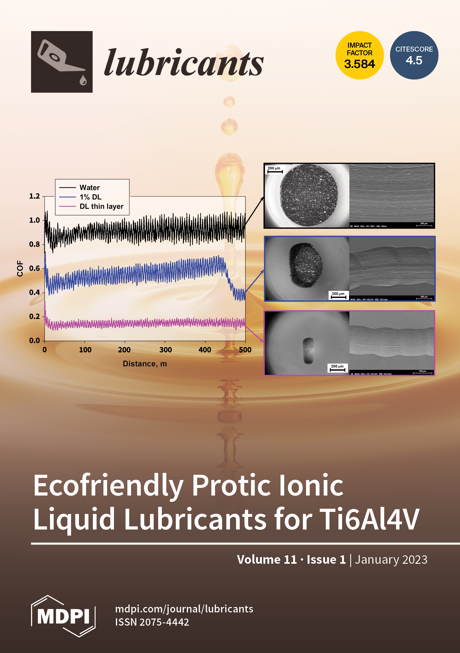
Skrzypek, Magdalena; Wojciechowski, Łukasz; Kałużny, Jarosław; Boncel, Sławomir; Marek, Adam A.; Runka, Tomasz; Nowicki, Marek; Jędrysiak, Rafał; Ruczka, Szymon; Błaszkiewicz, Paulina
Carbon Nanotubes Decorated with Nickel or Copper as Anti-Wear and Extreme-Pressure Additives for Greases Journal Article
In: Lubricants, vol. 12, pp. 448, 2024.
@article{Lubricants2024,

title = {Carbon Nanotubes Decorated with Nickel or Copper as Anti-Wear and Extreme-Pressure Additives for Greases},

author = {Magdalena Skrzypek and Łukasz Wojciechowski and Jarosław Kałużny and Sławomir Boncel and Adam A. Marek and Tomasz Runka and Marek Nowicki and Rafał Jędrysiak and Szymon Ruczka and Paulina Błaszkiewicz},

doi = {10.3390/lubricants12120448},

year  = {2024},

date = {2024-12-16},

journal = {Lubricants},

volume = {12},

pages = {448},

abstract = {To increase the anti-wear (AW) and anti-scuffing possibilities of commercially available lithium grease, this paper proposed enriching the original composition with functionalised carbon nanotubes (CNTs) at a concentration of 0.1% (w/w). The CNTs were modified by decorating them with nanoparticles of two metals with established tribological potential: copper and nickel. The AW and extreme-pressure properties were determined using the customised ISO-20623 test on a four-ball apparatus. The AW properties were determined using the standardised parameter MWSD (mean wear scar diameter) and the anti-scuffing properties using the last non-seizing load. The greases enriched with nanoadditives showed better AWproperties compared to the reference grease at higher loads (1–1.2 kN). Particularly favourable results were observed for grease with the addition of Cudecorated CNTs, for which the MWSD values were more than 50% lower than the reference. Optical microscopy, SEM and TEM microscopy with EDS analysis, and Raman spectroscopy were used to identify the wear mechanisms and characterise the role of nanoadditives in the lubrication process.},

keywords = {},

pubstate = {published},

tppubtype = {article}

}

Kałuziak, Piotr; Raczyński, Jan; El-Ahmar, Semir; Koczorowski, Wojciech
Study of InSb Thin Films obtained by imperfect method for nearly perfect applications Conference
Technolutions 2024, Warsaw, November 26-27, 2024, (Poster presentation).
@conference{Technol2024_PK,

title = {Study of InSb Thin Films obtained by imperfect method for nearly perfect applications},

author = {Piotr Kałuziak and Jan Raczyński and Semir El-Ahmar and Wojciech Koczorowski},

url = {https://nano.put.poznan.pl/wp-content/uploads/2024/12/Technolutions2024_PK.pdf},

year  = {2024},

date = {2024-11-26},

booktitle = {Technolutions 2024},

address = {Warsaw, November 26-27},

abstract = {Indium antimonide InSb is a III V group crystalline semiconductor with a room temperature energy gap of 0,18 eV a high electron mobility of 78 000 cm²/Vs hole mobility of 850 cm²/Vs which is crucial for efficient electronic devices This increased mobility leads to faster response times in infrared ( photodetectors, improving sensitivity and operational speed. InSb thin films can be grown on gallium arsenide substrates using Molecular Beam Epitaxy (MBE). MBE enhances film quality through precise deposition control, including environmental regulation, atomic layer deposition, flux monitoring, temperature control and the use of intermediate layers. Lately the MBE method was improved, which his resulted in more homogeneous InSb films In these studies, it was decided to use the less perfect Flash Evaporation Method (FEM). FEM does not fabricate layers of such good quality as MBE, but it is a cheaper and less demanding method, and what is more, the resulting layer imperfections may have potential applications in cybersecurity as physical unclonable functions(PUF). The studies presented here lead to the determination of the measurability and usability of fabrication defects in future plans to use them as cybersecurity elements.


Funding from the Ministry of Education and Science (Poland), Project No. 0512/SBAD/2420 and 0512/SBAD/6217

Funding from the National Centre for Research and Development (Poland), Project “MAGSET” No. LIDER/8/0021/L- 11/19/NCBR/2020},

note = {Poster presentation},

keywords = {},

pubstate = {published},

tppubtype = {conference}

}
Funding from the Ministry of Education and Science (Poland), Project No. 0512/SBAD/2420 and 0512/SBAD/6217
Funding from the National Centre for Research and Development (Poland), Project “MAGSET” No. LIDER/8/0021/L- 11/19/NCBR/2020
Ciuk, Tymoteusz; Nouvellon, Corinne; Monteverde, Fabien; Stańczyk, Beata; Przyborowska, Krystyna; Czołak, Dariusz; El-Ahmar, Semir
High-temperature Thermal Stability of a Graphene Hall Effect Sensor on Defect-engineered 4H-SiC(0001) Journal Article
In: IEEE Electron Device Letters, vol. 45, no. 10, pp. 1957-1960, 2024.
@article{EDL2024,

title = {High-temperature Thermal Stability of a Graphene Hall Effect Sensor on Defect-engineered 4H-SiC(0001)},

author = {Tymoteusz Ciuk and Corinne Nouvellon and Fabien Monteverde and Beata Stańczyk and Krystyna Przyborowska and Dariusz Czołak and Semir El-Ahmar},

doi = {10.1109/LED.2024.3436050},

year  = {2024},

date = {2024-09-30},

urldate = {2024-09-30},

journal = {IEEE Electron Device Letters},

volume = {45},

number = {10},

pages = {1957-1960},

abstract = {In this letter, we demonstrate a Hall effect sensor in the technology of amorphous-Al 2 O 3 -passivated transfer-free p-type hydrogen-intercalated quasi-free-standing epitaxial Chemical Vapor Deposition graphene on semi-insulating high-purity on-axis 4H-SiC(0001), pre-epitaxially modified with 5-keV hydrogen (H + ) ions. The sensor operates between 305 K and 770 K, with a current-mode sensitivity of ~75 V/AT and thermal stability below 0.15 %/K (⩽ 0.03 %/K in a narrower range between 305 K and 700 K). It is a promising two-dimensional platform for high-temperature magnetic diagnostics and plasma control systems for modern tokamak fusion reactors.


Funding from the Ministry of Education and Science (Poland), Project No. 0512/SBAD/2420},

keywords = {},

pubstate = {published},

tppubtype = {article}

}
Funding from the Ministry of Education and Science (Poland), Project No. 0512/SBAD/2420

Koczorowski, Wojciech; Raczyński, Jan
Comparative investigation of PtSe2-based systems from 1L to bulk Conference
IWSP, Niemcza, September 22-26, 2024, (Oral presentation).
@conference{IWSP2024_WK,

title = {Comparative investigation of PtSe2-based systems from 1L to bulk},

author = {Wojciech Koczorowski and Jan Raczyński},

url = {https://nano.put.poznan.pl/wp-content/uploads/2024/09/IWSP2024_WK.pdf},

year  = {2024},

date = {2024-09-23},

booktitle = {IWSP},

address = {Niemcza, September 22-26},

abstract = {The Transition Metal Dichalcogenides (TMD) class of materials attracts the interest of researchers and technologists because of their intrinsic physical properties, such as the thickness dependence of electronic properties that switch from semiconducting to metallic in the same material and the possibility of bandgap engineering. PtSe2 is a promising material with potential for future applications due to the chemical stability of the surface and the predicted high charge carrier mobility. In the presentation experimental studies of 1, 2, 3, 5, and 10 L of PtSe2 deposited on an Al2O3 substrate will be shown, including a comparison with the bulk properties. The discussion will focus on the properties of commercially available samples and the impact of temperature on the considered systems (in the range of RT to 520K). Finally, the fabrication of elaborate procedures for the PtSe2-based simple electronic devices will be discussed.


Funding from the Ministry of Education and Science (Poland), Project No. 0512/SBAD/2420

Funding from the National Science Centre (Poland), Project No. 2019/35/O/ST5/01940},

note = {Oral presentation},

keywords = {},

pubstate = {published},

tppubtype = {conference}

}
Funding from the Ministry of Education and Science (Poland), Project No. 0512/SBAD/2420
Funding from the National Science Centre (Poland), Project No. 2019/35/O/ST5/01940
Raczyński, Jan; Koczorowski, Wojciech
Comparison of different metal/PtSe2 systems Conference
IWSP, Niemcza, September 22-26, 2024, (Oral presentation).
@conference{IWSP2024_JR,

title = {Comparison of different metal/PtSe2 systems},

author = {Jan Raczyński and Wojciech Koczorowski},

url = {https://nano.put.poznan.pl/wp-content/uploads/2024/09/IWSP2024_JR.pdf},

year  = {2024},

date = {2024-09-23},

urldate = {2024-09-23},

booktitle = {IWSP},

address = {Niemcza, September 22-26},

abstract = {Today, 2D materials also include Transition Metal Dichalcogenides (TMD), which provide a wide range of charge carrier mobility values and bandgap energy, which depend on the thickness. One of the most promising TMD materials for further applications is PtSe2, which exhibits a chemically nonreactive surface, it is crucial to determine the properties of the metal/PtSe2 interfaces. Different metals form morphologically unique structures on the PtSe2 surface, which requires a comprehensive analysis of physicochemical properties including an analysis of the thermal stability of such systems. This presentation will discuss the properties of the metallic layers (eg. Ni, Ti) with various thicknesses embedded on the surface of the bulk PtSe2 crystal. Particular emphasis will be placed on forming intermixed phases at the interface observed in the form of vibration modes in Raman spectroscopy and the chemical shift in XPS measurements. The observed differences between the metal layer and PtSe2 indicate the distinctive properties of such structures, which translate into the operation of planar architecture sensor devices.


Funding from the Ministry of Education and Science (Poland), Project No. 0512/SBAD/2320

Funding from the National Science Centre (Poland), Project No. 2019/35/O/ST5/01940, NAWA grant No.PPN/STA/2021/1/00043},

note = {Oral presentation},

keywords = {},

pubstate = {published},

tppubtype = {conference}

}
Funding from the Ministry of Education and Science (Poland), Project No. 0512/SBAD/2320
Funding from the National Science Centre (Poland), Project No. 2019/35/O/ST5/01940, NAWA grant No.PPN/STA/2021/1/00043
Kwiecień, Katarzyna; Raczyński, Jan; Puchalska, Agnieszka; Nowak, Ewelina; Chłopocka, Edyta; Kot, Damian; Szybowicz, Mirosław; Jurczyszyn, Leszek; Koczorowski, Wojciech
The effects of short-term air exposure of monocrystal HfSe2 surface Conference
IWSP, Niemcza, September 22-26, 2024, (Oral presentation).
@conference{IWSP2024_KK,

title = {The effects of short-term air exposure of monocrystal HfSe2 surface},

author = {Katarzyna Kwiecień and Jan Raczyński and Agnieszka Puchalska and Ewelina Nowak and Edyta Chłopocka and Damian Kot and Mirosław Szybowicz and Leszek Jurczyszyn and Wojciech Koczorowski},

url = {https://nano.put.poznan.pl/wp-content/uploads/2024/09/IWSP2024_KK.pdf},

year  = {2024},

date = {2024-09-23},

booktitle = {IWSP},

address = {Niemcza, September 22-26},

abstract = {One of the ways to improve silicon-based electronics is the integration of silicon with a material that possesses properties such as a sizable band gap (Eg) in the range of 1 - 2 eV and high room temperature carrier mobility (RTCM). HfSe2, which belongs to transition metal dichalcogenides (TMDs) group, is a material that meets these requirements. Predicted RTCM of HfSe2 is the highest among TMDs (3500 cm2 V-1 s-1). Its bulk Eg is 1.1 eV and depends on the number of its layers and on the presence of HfO2 in its subsurface, which widens the Eg up to 2 eV. Due to the sensitivity of HfSe2 to oxidation and its technological importance in possible future applications, we investigated this process for exfoliated bulk HfSe2 crystal under ambient conditions. Our scanning electron microscopy studies show early oxidation with a rapid increase in the Se-rich blister coverage. X-ray photoemission data reveals diffusion of O atoms into the bulk and HfO2 formation. Raman spectroscopy results confirm the coexistence of HfSe2 and HfO2 on the surface. Additionally, we confront the experimental findings with the density functional theory predictions.


Funding from the Ministry of Education and Science (Poland), Project No. 0512/SBAD/2420 and 0612/SBAD/6215},

note = {Oral presentation},

keywords = {},

pubstate = {published},

tppubtype = {conference}

}
Funding from the Ministry of Education and Science (Poland), Project No. 0512/SBAD/2420 and 0612/SBAD/6215
Koczorowski, Wojciech; Raczyński, Jan; Kwiecień, Katarzyna; Czajka, Ryszard
Charakteryzacja wybranych materiałów TMD zawierających Se Conference
XIII Konferencja Techniki Próżni, Warsaw, September 19-20, 2024, (Invited lecture).
@conference{PTP2024_WK,

title = {Charakteryzacja wybranych materiałów TMD zawierających Se},

author = {Wojciech Koczorowski and Jan Raczyński and Katarzyna Kwiecień and Ryszard Czajka},

url = {https://nano.put.poznan.pl/wp-content/uploads/2024/09/XIIIKTP-WK.pdf},

year  = {2024},

date = {2024-09-20},

urldate = {2024-09-20},

booktitle = {XIII Konferencja Techniki Próżni},

address = {Warsaw, September 19-20},

abstract = {Dichalkogenki metali przejściowych (TMD) to grupa materiałów dwuwymiarowych, które posiadają ciekawe właściwości fizyczne. Wykazują one silną zależność właściwości elektronowych w funkcji ilości ultra-cienkich warstw (od jednej do kilku ML). Pozwala to uzyskać zarówno charakterystykę półprzewodnikową jak i metaliczną dla tego samego materiału. Powoduje to, że materiały TMD podlegają intensywnym badaniom naukowym. W ramach prezentacji pokazane zostaną wyniki prac eksperymentalnych dotyczących PtSe2 oraz HfSe2, które cechują się dużą wartością ruchliwości nośników ładunków elektrycznych. Istotną cechą różnicującą te materiały jest ich aktywność chemiczna, która jest znacznie większa w przypadku HfSe2. W przypadku PtSe2 główny nacisk postawiony zostanie na analizie widm spektroskopii Ramana (RS) umożliwiającej jednoznaczne określenie ilości ML w układzie. Dla powierzchni kryształu HfSe2 omówione zostaną komplementarne wyniki uzyskane za pomocą technik: skaningowej mikroskopii elektronowej (SEM), rentgenowskiej spektrometrii fotoelektronów (XPS) i RS prezentujące zmiany morfologii warstw przypowierzchniowych, które są efektem ekspozycji na warunki zewnętrzne oraz umożliwiają zrozumienie dynamiki procesu utleniania powierzchni. W końcowej części zaprezentowana zostanie także metoda strukturyzacji prostych urządzeń elektronowych z wykorzystaniem: litografii optycznej, strukturyzowania plazmą argonową oraz osadzania warstw metalicznych z wykorzystaniem osadzania magnetronowego.


Funding from the Ministry of Education and Science (Poland), Project No. 0512/SBAD/2420

Funding from the National Science Center (Poland), Project No. 2019/35/O/ST5/01940},

note = {Invited lecture},

keywords = {},

pubstate = {published},

tppubtype = {conference}

}
Funding from the Ministry of Education and Science (Poland), Project No. 0512/SBAD/2420
Funding from the National Science Center (Poland), Project No. 2019/35/O/ST5/01940

El-Ahmar, Semir; Reddig, Wiktoria; Jagiełło, Jakub; Szary, Maciej J.; Dobrowolski, Artur; Prokopowicz, Rafał; Ziemba, Maciej; Wzorek, Marek; Ciuk, Tymoteusz
Graphene & 2D Mat. 9, Poznan, September 8-10, 2024, (Invited lecture).
@conference{GR2DMAT9_SA,

title = {Exploring the limits of graphene's operation in extreme conditions imposed by the future energy industry},

author = {Semir El-Ahmar and Wiktoria Reddig and Jakub Jagiełło and Maciej J. Szary and Artur Dobrowolski and Rafał Prokopowicz and Maciej Ziemba and Marek Wzorek and Tymoteusz Ciuk},

url = {https://nano.put.poznan.pl/wp-content/uploads/2024/09/GR2DMat9_SA.pdf},

year  = {2024},

date = {2024-09-10},

booktitle = {Graphene & 2D Mat. 9},

address = {Poznan, September 8-10},

abstract = {Our research explores the potential of using two-dimensional (2D) carbon structures as magnetic field detectors capable of operating in the extreme conditions of future thermonuclear power plants. In so-called magnetic-confinement fusion reactors, electronics will be exposed to high temperatures and radiation damage. We demonstrate the experimental study on the impact of neutron radiation and determine its influence on the electrical parameters of epitaxial graphene-based systems. We have conducted preliminary research to investigate the impact of high temperature and neutron irradiation separately. For this purpose, we fabricated a hydrogen-intercalated quasi-free-standing (QFS) graphene on semi-insulating 4H-SiC(0001) and 6H-SiC(0001), passivated with an Al2O3 layer [3,4]. The systems were exposed to highenergy neutron fluxes using the MARIA research nuclear reactor. We theorize that the main factor affecting the QFS properties of graphene in tested systems is the depletion of atoms in the hydrogen layer, based on Hall effect measurements and micro-Raman characterization supported by high-resolution transmission electron microscopy. We have predicted, using density functional theory calculations, that damage to the intercalation lowers carrier concentration in graphene. We anticipate that temperatures above 200°C will facilitate the diffusion of the hydrogen atoms from parts with higher to lower concentrations. This effect can reduce the surface area where intercalation is too low to support the separation of the graphene and improve its QFS properties.

Understanding the mechanism of damaging the tested systems by neutron radiation is a key milestone in assessing its suitability for magnetic field detection in harsh environments.


Funding from the Ministry of Education and Science (Poland), Project No. 0512/SBAD/2420},

note = {Invited lecture},

keywords = {},

pubstate = {published},

tppubtype = {conference}

}
Understanding the mechanism of damaging the tested systems by neutron radiation is a key milestone in assessing its suitability for magnetic field detection in harsh environments.
Funding from the Ministry of Education and Science (Poland), Project No. 0512/SBAD/2420