 WHAT WE DO?
In short, we explore the surface of solids with sub-nanometer resolution! This allows us to determine the atomic structure of the investigated surfaces, to analyze their electronic properties as well as to obtain a range of other information and statistical data. Following the leading trends in science, in recent years we have focused mainly on the so-called systems of reduced dimension, such as ultra-thin films, sub-monolayers, nanowires and nanoclusters, and molecular structures.
For surface studies, we use scanning tunneling microscopes (STM) and atomic force microscopes (AFM), and additionally, with the help of tunneling spectroscopy, we create maps of the local density of states. The STM and AFM microscopes in our laboratories are adapted to work in ultra-high vacuum (UHV) conditions in a wide temperature range from 4.2 K to 600 K. We also use techniques of low-energy electron diffraction (LEED) and Auger electron spectroscopy (AES) as well as many other research techniques available at our faculty, such as scanning electron microscopy (SEM), infrared, visible, and ultraviolet absorption spectroscopy (IR&UV -Vis) or resonant Raman scattering (RRS).
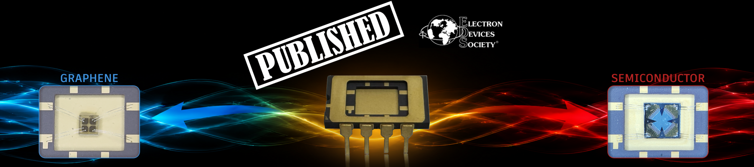
An important application of systems of reduced dimension is nanosensors, e.g. using graphene as an active element. We test and modify the properties of materials in such a way as to enable their use in magnetic field sensors capable of stable operation in extreme environments.