
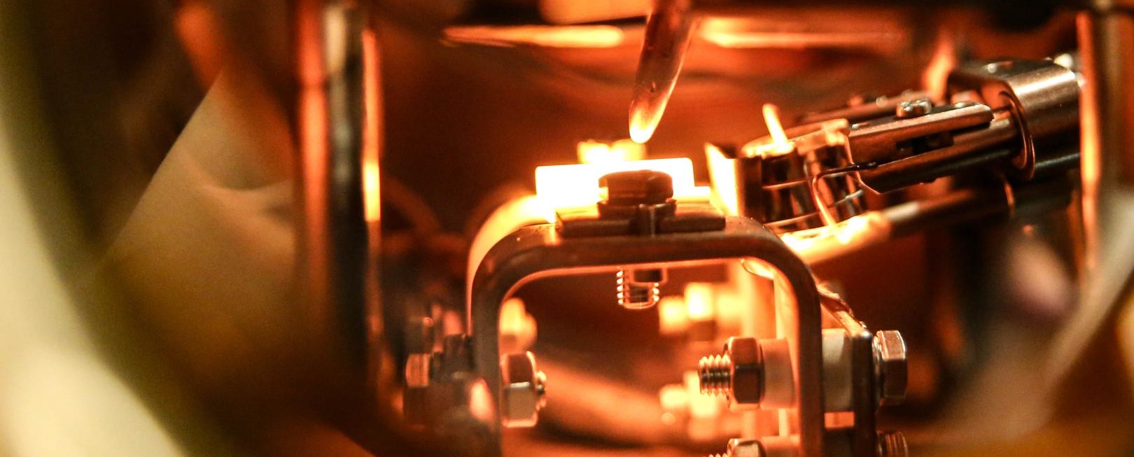
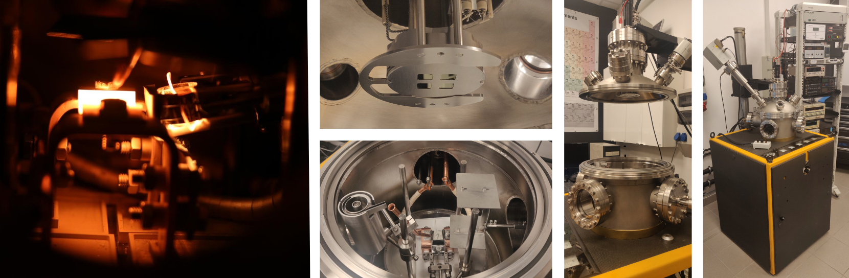
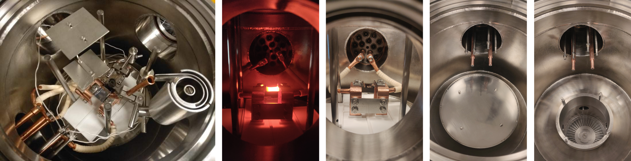
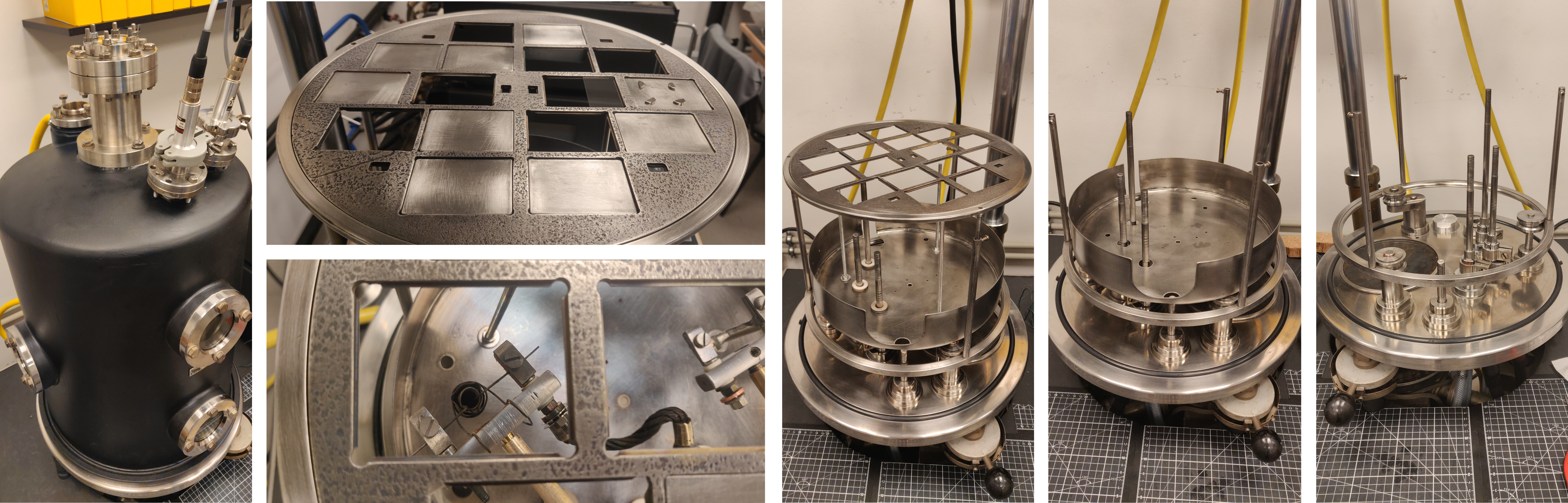
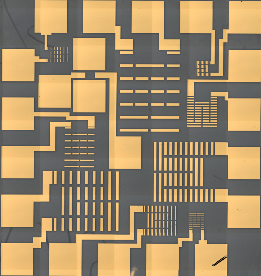
We are equipped with a unique vacuum apparatus for the production of thin semiconductor, metallic and insulating layers. We very often build our equipment ourselves, adjusting its capabilities to our needs.
The main techniques we use to produce thin films are the flash evaporation method and physical vapor deposition.
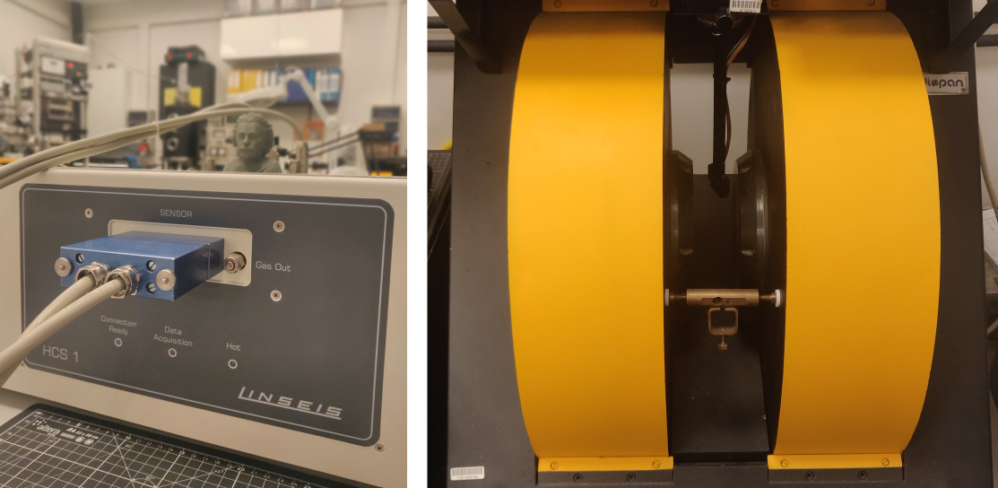
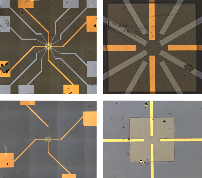
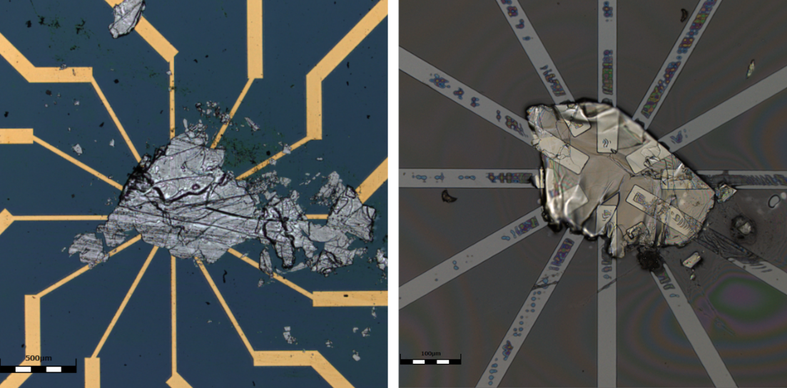
We have the possibility of electric characterization of the produced materials thanks to the equipment for conducting galvanomagnetic measurements. In our laboratory, we have 2 independent measuring systems at our disposal: a stand equipped with an electromagnet (0 T – 1 T), and the ![]() stand equipped with a permanent magnet (0.7 T). Both systems enable measurements of the Hall effect in a wide temperature range (115 K – 825 K).
stand equipped with a permanent magnet (0.7 T). Both systems enable measurements of the Hall effect in a wide temperature range (115 K – 825 K).

 The response of the graphene/SiC system to strong neutron radiation
Exploring the limits of indium antimonide toward the development of magnetic field sensors for extreme environments
![]() MAGSET, LIDER/8/0021/L-11/19/NCBR/2020, Magnetic field sensors for industrial applications in extreme temperature ranges
MAGSET, LIDER/8/0021/L-11/19/NCBR/2020, Magnetic field sensors for industrial applications in extreme temperature ranges
![]() UMO-2012/07/N/ST5/00207, Investigation of the influence of neutron irradiation on the electrical properties of InGaSb thin films
UMO-2012/07/N/ST5/00207, Investigation of the influence of neutron irradiation on the electrical properties of InGaSb thin films
![]() 7th FP EU, Development of high-temperature Hall sensors for future applications in the measurement of the magnetic field in fusion reactors
7th FP EU, Development of high-temperature Hall sensors for future applications in the measurement of the magnetic field in fusion reactors
Investigation of physical properties of two-dimensional structures and layered materials for applications in magnetic field detection
![]() 2019/35/O/ST5/01940, Investigation of the physical properties of thin-film metal / PtSe2 interfaces
2019/35/O/ST5/01940, Investigation of the physical properties of thin-film metal / PtSe2 interfaces
![]() GRAFMAG, GRAF-TECH/NCBR/12/14/2013, Graphene magnetic field sensors for industrial applications. Task: Fabrication of a graphene EMR sensor for the needs of a current transformer
GRAFMAG, GRAF-TECH/NCBR/12/14/2013, Graphene magnetic field sensors for industrial applications. Task: Fabrication of a graphene EMR sensor for the needs of a current transformer
Exploring the planar configuration of extraordinary magnetoresistance
![]() UMO-2012/07/N/ST8/03911, Modeling the phenomenon of Extraordinary Magnetoresistance in newly developed hybrid metal-semiconductor structures using the Finite Element Method
UMO-2012/07/N/ST8/03911, Modeling the phenomenon of Extraordinary Magnetoresistance in newly developed hybrid metal-semiconductor structures using the Finite Element Method
Development of the concept of reducing the voltage offset of the Hall sensor
![]()


![]()