Faculty of Materials Engineering and Technical Physics
POZNAN UNIVERSITY of TECHNOLOGY
EDU LAB
EDU LAB is the collective name of two independent laboratories that share a common space: the SPM Laboratory and the Nanomechanical Measurement Laboratory
We conduct research here mainly towards the implementation of thematic diploma theses by students of Technical Physics and Education in Technology and Informatics. It is also here that specialized laboratories in the field of nanotechnology and nanomechanics are held.
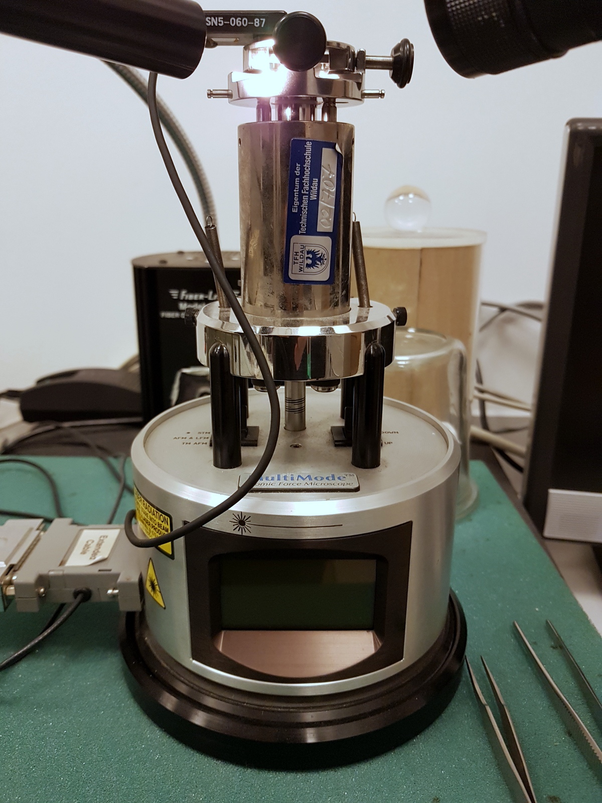
In the laboratory, it is possible to measure the surface topography of solids and nanostructures on the nanometer and sub-nanometer scale (with atomic resolution) using a scanning tunneling microscope (STM) under gas atmosphere conditions.
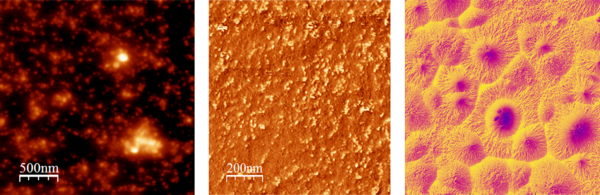
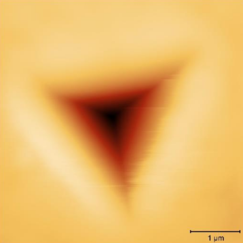
The work currently carried out at the SPM LABORATORY focuses on the study of objects such as carbon nanotubes or silver nanoparticles. We also carry out nano- and micro-lithography on selected surfaces, e.g. topological insulators such as Bi2Te3 or Sb2Te3.
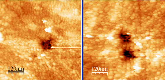
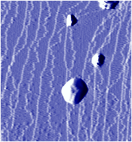
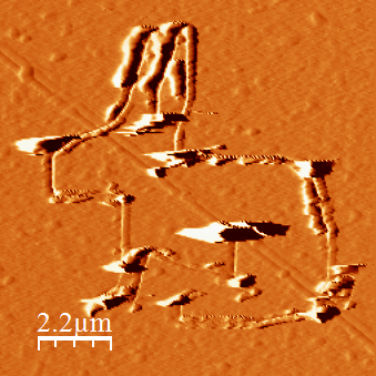
The atomic force microscope (AFM) allows us to imagine and analyze the surface structure of the vast majority of materials used in the industry. It is possible to test the homogeneity, the degree of coverage of one material with the other, and the thickness of thin layers. The roughness of samples can be determined with nanometer accuracy (e.g. roughness of coatings used in optics).
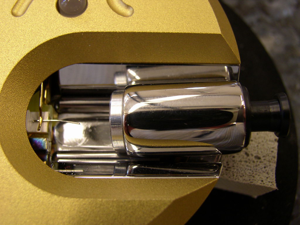
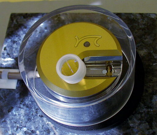
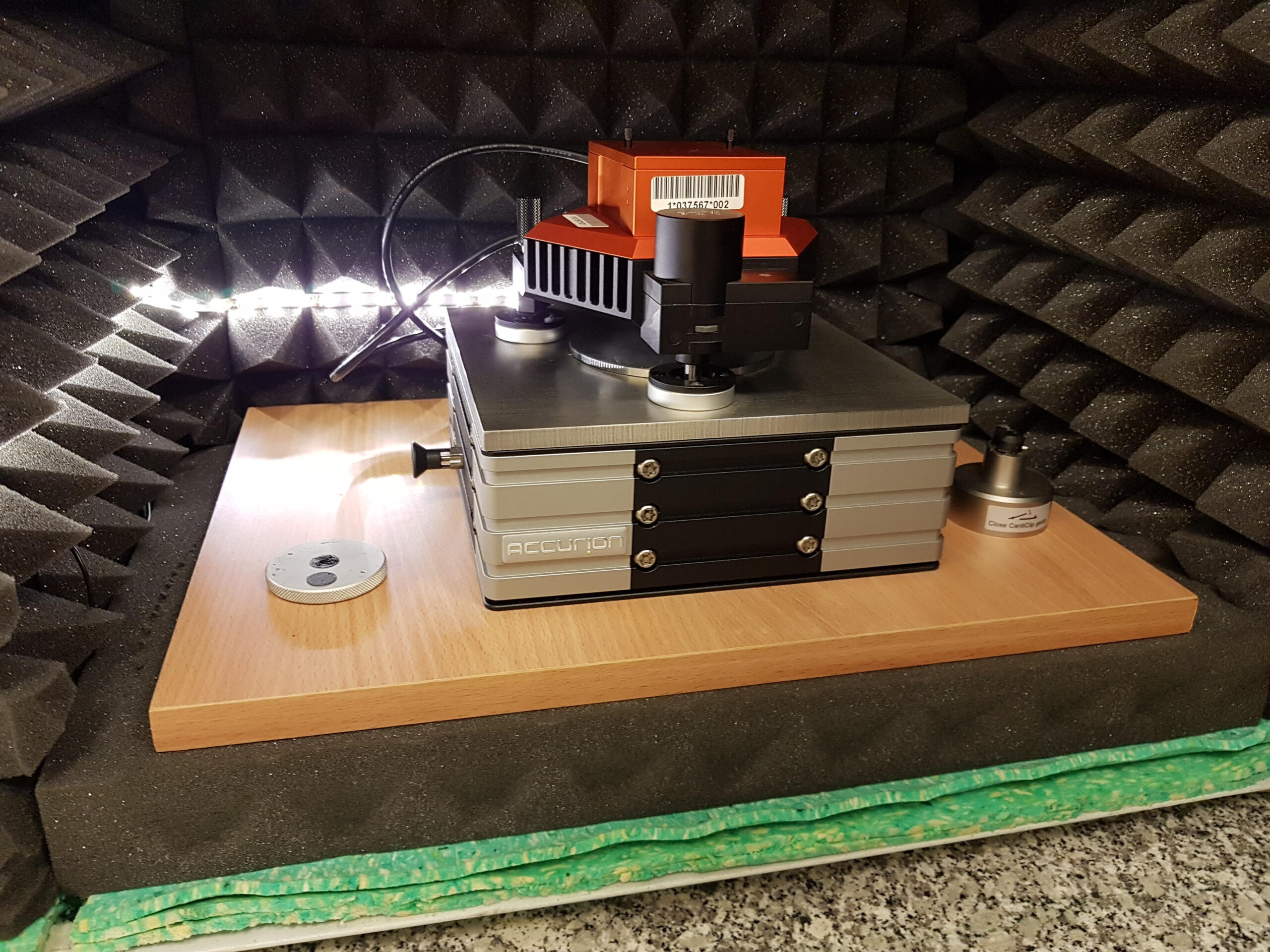
The laboratory is equipped with 2 atomic force microscopes (AFM) and a device for measuring indentation, the so-called indenter.
Using the AFM microscopes, we can study the surface topography of materials with sub-nanometer resolution. Our AFM microscopes enable measurements in many operating modes (contact, intermittent contact, force modulation, magnetic, electric), and also in liquids.
Thanks to the indenter, we are able to measure the indentation of the probe into the surface of the tested material. The place of such measurement can be selected with nanometer precision thanks to the use of the AFM piezoelectric scanner. Thanks to indentation measurements, we can determine the local hardness and modulus of elasticity of the tested material.

 Introduction to nanotechnology – template for the report
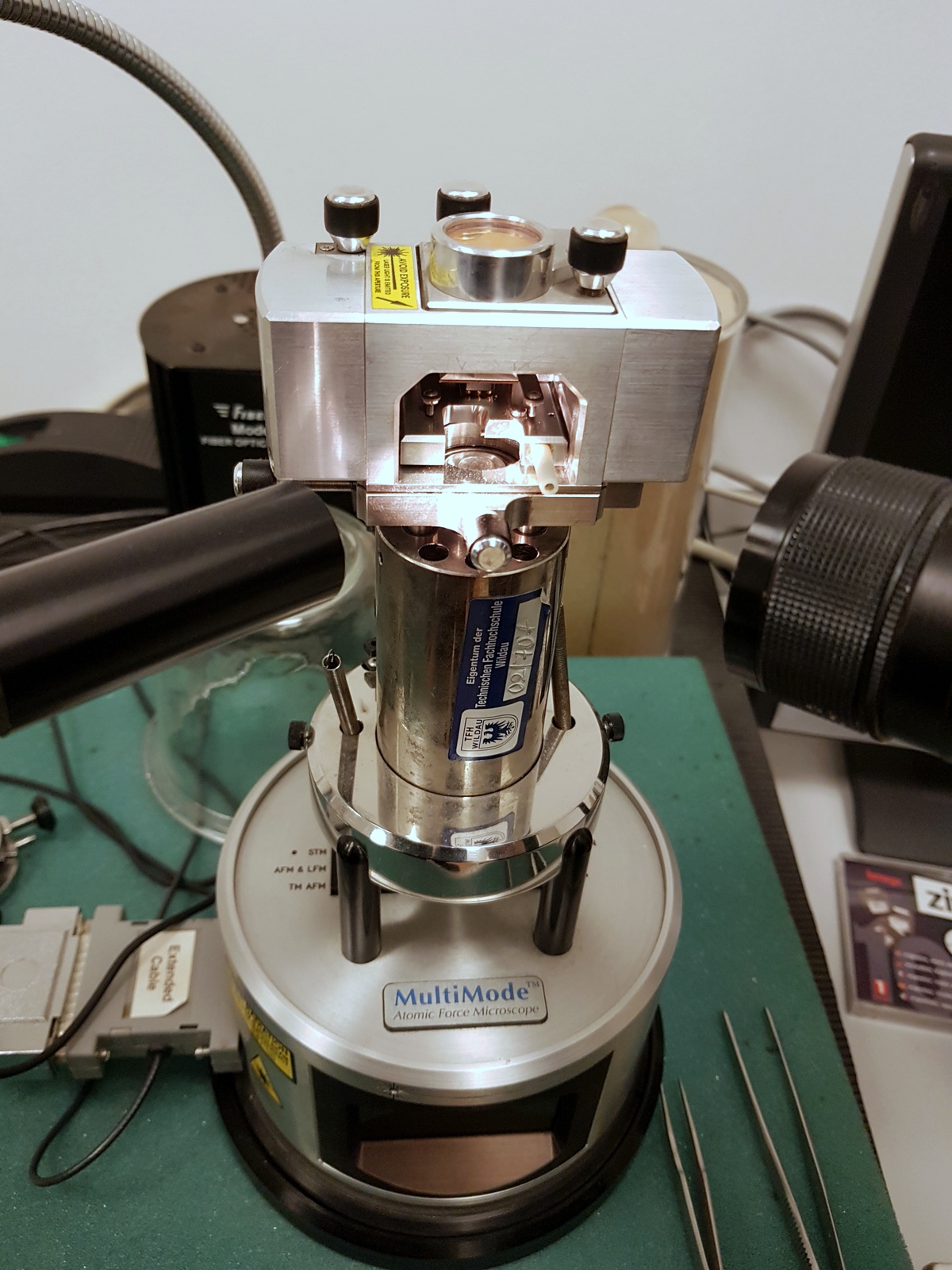